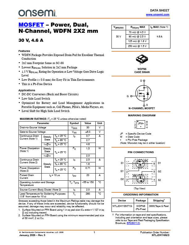
NTLJD4116N
NTLJD4116N is Dual N-Channel MOSFET manufactured by onsemi.
Features
- WDFN Package Provides Exposed Drain Pad for Excellent Thermal
Conduction
- 2x2 mm Footprint Same as SC-88
- Lowest RDS(on) Solution in 2x2 mm Package
- 1.5 V RDS(on) Rating for Operation at Low Voltage Gate Drive Logic
Level
- Low Profile (< 0.8 mm) for Easy Fit in Thin Environments
- This is a Pb-Free Device
Applications
- DC-DC Converters (Buck and Boost Circuits)
- Low Side Load Switch
- Optimized for Battery and Load Management Applications in
Portable Equipment such as, Cell Phones, PDA’s, Media Players, etc.
- Level Shift for High Side Load Switch
MAXIMUM RATINGS (TJ = 25 C unless otherwise noted)
Parameter
Symbol Value Unit
Drain-to-Source Voltage
VDSS
Gate-to-Source Voltage
8.0
Continuous Drain Steady TA = 25 C
Current (Note 1)
State TA = 85 C
2.7 t 5 s TA = 25 C
Power Dissipation Steady
(Note 1)
State TA = 25 C t 5 s
Continuous Drain
TA = 25...