NTTS2P02R2
NTTS2P02R2 is Power MOSFET manufactured by onsemi.
Features
- -
- -
- -
Ultra Low RDS(on) Higher Efficiency Extending Battery Life Logic Level Gate Drive Miniature Micro- 8 Surface Mount Package Diode Exhibits High Speed, Soft Recovery Micro8 Mounting Information Provided http://onsemi.
Applications
- Power Management in Portable and Battery- Powered Products, i.e.:
Cellular and Cordless Telephones and PCMCIA Cards
MAXIMUM RATINGS (TJ = 25°C unless otherwise noted)
Rating Drain- to- Source Voltage Gate- to- Source Voltage
- Continuous Thermal Resistance
- Junction- to- Ambient (Note 1.) Total Power Dissipation @ TA = 25°C Continuous Drain Current @ TA = 25°C Continuous Drain Current @ TA = 70°C Pulsed Drain Current (Note 3.) Thermal Resistance
- Junction- to- Ambient (Note 2.) Total Power Dissipation @ TA = 25°C Continuous Drain Current @ TA = 25°C Continuous Drain Current @ TA = 70°C Pulsed Drain Current (Note 3.) Operating and Storage Temperature Range Single Pulse Drain- to- Source Avalanche Energy
- Starting TJ = 25°C (VDD =
- 20 Vdc, VGS =
- 4.5 Vdc, Peak IL =
- 5.0 Apk, L = 28 m H, RG = 25 Ω) Maximum Lead Temperature for Soldering Purposes for 10 seconds Symbol VDSS VGS RθJA PD ID ID IDM RθJA PD ID ID IDM TJ, Tstg EAS Value
- 20 ±8.0 Unit V V
- 2.4 AMPERES
- 20 VOLTS RDS(on) = 90 m W
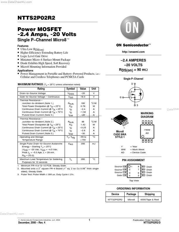
Single P- Channel D
160 °C/W 0.78 W
- 2.4 A
- 1.92 A
- 20 A . 88 1.42
- 3.25
- 2.6
- 30
- 55 to +150 350 °C/W W A A A °C m J Y WW AD 8
Data Shee
MARKING DIAGRAM
1 Micro8 CASE 846A STYLE 1
YWW AD
= Year = Work Week = Device Code
°C Source Source Source Gate
PIN ASSIGNMENT
1 2 3 4 8 7 6 5 Drain Drain Drain Drain
1. Minimum FR- 4 or G- 10 PCB, Steady State. 2. Mounted onto a 2″ square FR- 4 Board (1″ sq. 2 oz Cu 0.06″ thick single sided), Steady State. 3. Pulse Test: Pulse Width ≤ 300 ms, Duty Cycle ≤...