NUS6160MN
NUS6160MN is Low Profile Overvoltage Protection manufactured by onsemi.
Features
- Overvoltage Turn- Off Time of Less Than 1.5 ms
- Undervoltage Lockout Protection; 3.0 V, Nominal
- High Accuracy Undervoltage Threshold of 5.0%
- - 20 V Integrated P- Channel Power MOSFET
- Low RDS(on) = 64 m W @
- 4.5 V
- pact 3.0 x 4.0 mm QFN Package
- Maximum Solder Reflow Temperature @ 260°C
- This is a Pb- Free Device
Benefits
- Provide Battery Protection
- Integrated Solution Offers Cost and Space Savings
- Integrated Solution Improves System Reliability
- Optimized for mercial PMUs from Top Suppliers
Applications
- Portable puters and PDAs
- Cell Phones and Handheld Products
- Digital Cameras http://onsemi.
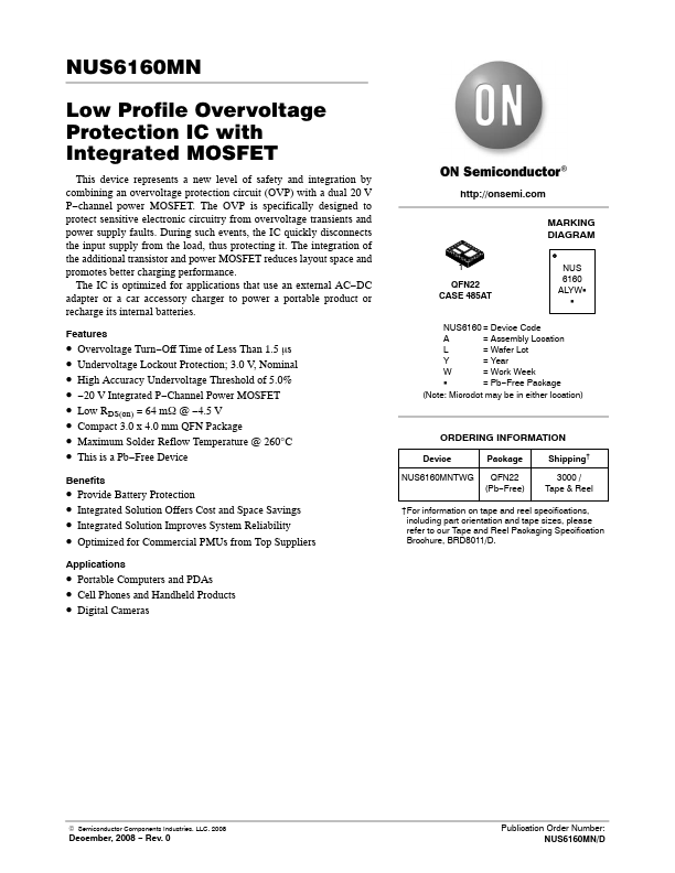
MARKING DIAGRAM
QFN22 CASE 485AT
NUS 6160 ALYWG
NUS6160 = Device Code
= Assembly Location
= Wafer Lot
= Year
= Work Week
= Pb- Free Package
(Note: Microdot may be in either location)
ORDERING INFORMATION
Device
Package
Shipping†...