P2N2907A Overview
Key Specifications
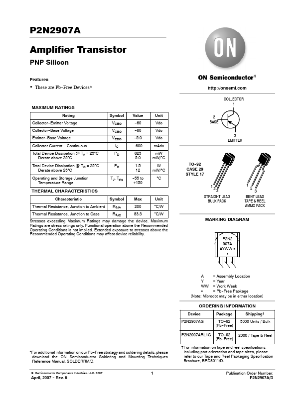
Package: TO-92-3
Mount Type: Through Hole
Pins: 3
Max Operating Temp: 150 °C
Key Features
- These are Pb--Free Devices*
| Part | P2N2907A |
|---|---|
| Description | Amplifier Transistor |
| Category | Transistor |
| Manufacturer | onsemi |
| Size | 158.35 KB |
Package: TO-92-3
Mount Type: Through Hole
Pins: 3
Max Operating Temp: 150 °C
| Seller | Inventory | Price Breaks | Buy |
|---|---|---|---|
| Verical | 8000 | 6834+ : 0.0549 USD 10000+ : 0.0489 USD 100000+ : 0.041 USD |
View Offer |
| Rochester Electronics | 8000 | 100+ : 0.0529 USD 500+ : 0.0476 USD 1000+ : 0.0439 USD 10000+ : 0.0391 USD |
View Offer |
| Part Number | Manufacturer | Description |
|---|---|---|
| P2N2907A | Motorola Semiconductor | Amplifier Transistor |
| P2N2907A | Continental Device India | PNP Silicon Transistor |
| P2N2907 | Continental Device India | PNP SILICON PLANAR EPITAXIAL TRANSISTORS |
| P2N2907 | Motorola Semiconductor | AMPLIFIER TRANSISTORS |