Datasheet Summary
Ordering number : ENA0520A
Excellent Power Device
Dual buffer driver for general purpose, Dual VEC8
Features
Dual buffer Monolithic structure (High voltage CMOS process adopted)
- Withstand voltage of 25V is assured
- Wide range of operating voltage : 4.5V to 25V
- Peak output current : IO+/IO--=0.8A /1A
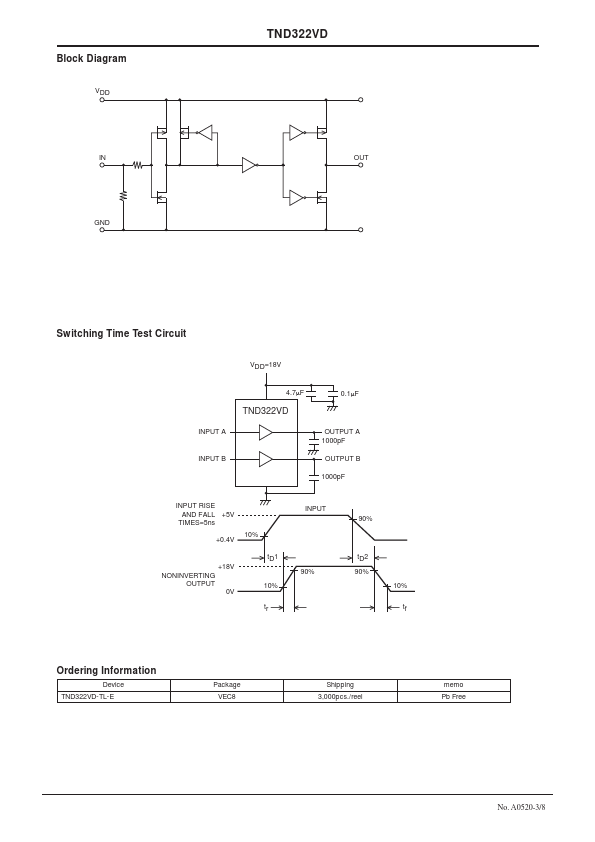
- Fast switching time (30ns typical at 1000pF load)
- Fully patible input to TTL / CMOS (VIH=up to 2.6V, at VDD=4.5 to 25V)
- Built-in input pull-down resistance
- - http://onsemi.
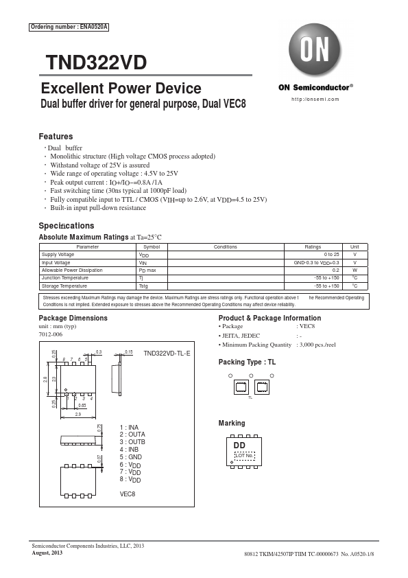
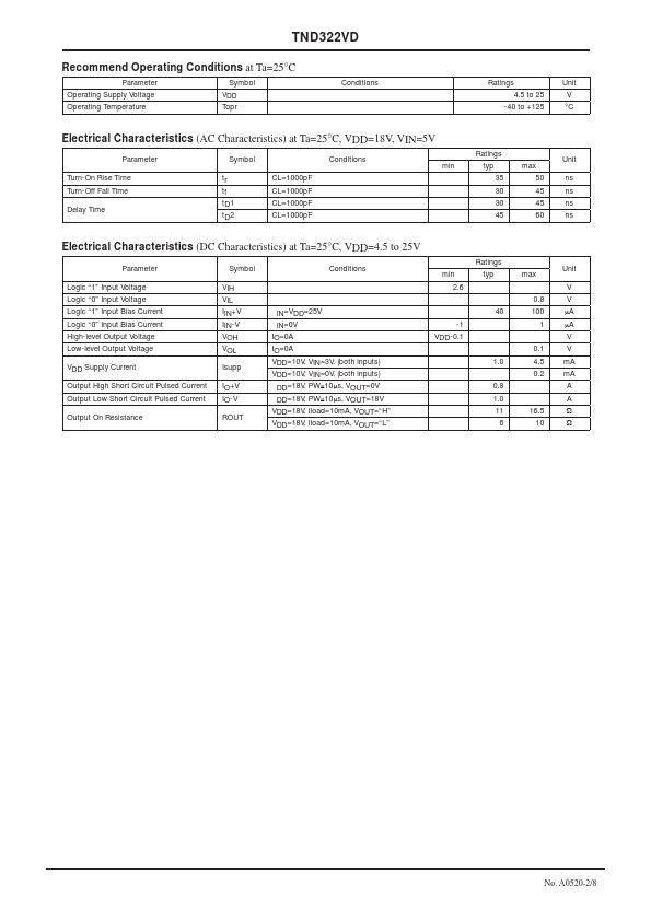
Specifications...