FDS6900AS-G Description
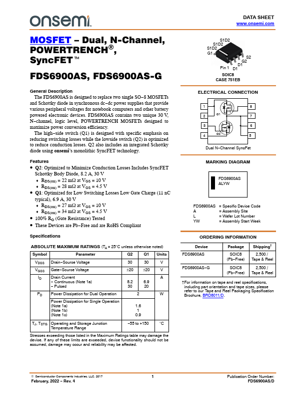
The FDS6900AS is designed to replace two single SO−8 MOSFETs and Schottky diode in synchronous dc−dc power supplies that provide various peripheral voltages for notebook puters and other battery powered electronic devices. FDS6900AS contains two unique 30 V, N−channel, logic level, POWERTRENCH MOSFETs designed to maximize power conversion efficiency. The high−side switch (Q1) is designed with specific emphasis on...
FDS6900AS-G Key Features
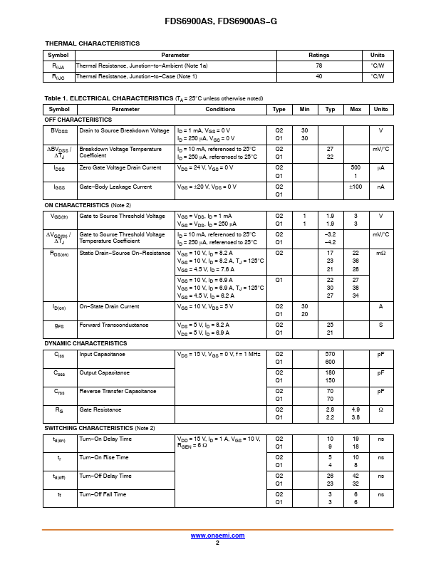
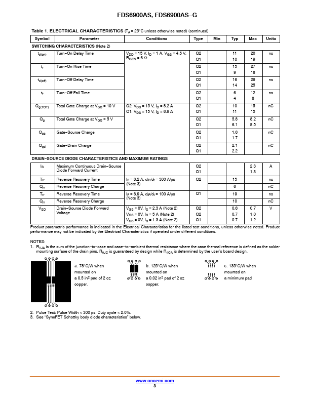
- Q2: Optimized to Minimize Conduction Losses Includes SyncFET
- RDS(on) = 22 mW at VGS = 10 V
- RDS(on) = 28 mW at VGS = 4.5 V
- Q1: Optimized for Low Switching Losses Low Gate Charge (11 nC
- RDS(on) = 27 mW at VGS = 10 V
- RDS(on) = 34 mW at VGS = 4.5 V
- 100% RG (Gate Resistance) Tested
- These Devices are Pb-Free and are RoHS pliant