2SD1249
Key Features
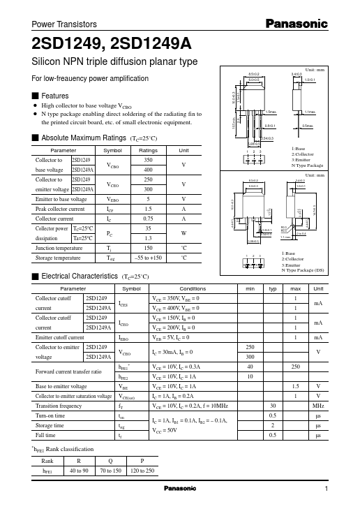
- 5min. High collector to base voltage VCBO N type package enabling direct soldering of the radiating fin to the printed circuit board, etc. of small electronic equipment. (TC=25˚C) Ratings 350 400 250 300 5 1.5 0.75 35 1.3 150 -55 to +150 Unit V
- 5max.
- 1max.
- 8±0.1
- 5max. s Absolute Maximum Ratings Parameter Collector to base voltage Collector to 2SD1249 2SD1249A 2SD1249 Symbol VCBO VCEO VEBO ICP IC PC Tj Tstg
- 54±0.3 5.08±0.5 1 2 3 1:Base 2:Collector 3:Emitter N Type Package Unit: mm
- 4±0.3 1.0±0.1
- 5±0.2 emitter voltage 2SD1249A Emitter to base voltage Peak collector current Collector current Collector power TC=25°C dissipation Ta=25°C Junction temperature Storage temperature V
- 0±0.3
- 0±0.3 V A A W