2SD2029
Key Features
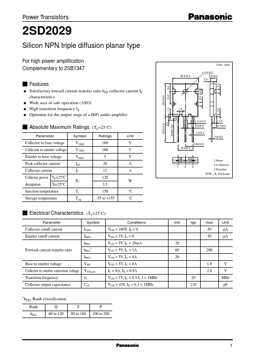
- 0±0.5
- 5 Solder Dip s Absolute Maximum Ratings Parameter Collector to base voltage Collector to emitter voltage Emitter to base voltage Peak collector current Collector current Collector power TC=25°C dissipation Ta=25°C Junction temperature Storage temperature Symbol VCBO VCEO VEBO ICP IC PC Tj Tstg
- 0±0.5 2.5
- 0±0.3 3.0±0.3 1.0±0.2
- 7±0.3
- 6±0.2 5.45±0.3 10.9±0.5 1 2 3 A W ˚C ˚C 1:Base 2:Collector 3:Emitter TOP-3L Package s Electrical Characteristics Parameter Collector cutoff current Emitter cutoff current (TC=25˚C) Symbol ICBO IEBO hFE1 hFE2* hFE3 VBE VCE(sat) fT Cob Conditions VCB = 160V, IE = 0 VEB = 3V, IC = 0 VCE = 5V, IC = 20mA VCE = 5V, IC = 1A VCE = 5V, IC = 8A VCE = 5V, IC = 8A IC = 8A, IB = 0.8A VCE = 5V, IC = 0.5A, f = 1MHz VCB = 10V, IE = 0, f = 1MHz 20 210 20 60 20 1.8 2.0 V V MHz pF 200 min typ max 50 50 Unit µA µA Forward current transfer ratio Base to emitter voltage Collector to emitter saturation voltage Transition frequency Collector output capacitance
- h FE2 Rank classification Q 60 to 120 S 80 to 160 P 100 to 200 Rank hFE2
- 0 1 Power Transistors PC - Ta