- Part: 2SD2067
- Description: Silicon NPN Transistor
- Category: Transistor
- Manufacturer: Panasonic
- Size: 54.77 KB
Key Features
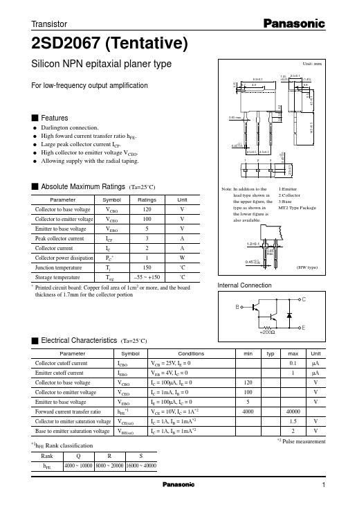
- 65 max.
- 0 1.0
- 2 Unit µA µA V V V VCE(sat) VBE(sat) V V Rank classification
Datasheets by Manufacturer
- 2SD2060 — Inchange Semiconductor — NPN Transistor
- 2SD2061 — ROHM — Power Transistor