2SD2249
Key Features
- 0 Parameter Collector to base voltage Collector to emitter voltage Emitter to base voltage Peak collector current Collector current Collector power dissipation Junction temperature Storage temperature * Symbol VCBO VCEO VEBO ICP IC PC* Tj Tstg Ratings 40 20 7 8 5 1 150 -55 ~ +150 1cm2 Unit V V V A A W ˚C ˚C 1 2 3
- 45-0.05 +0.1 s Absolute Maximum Ratings
- 45-0.05 +0.1 (Ta=25˚C)
- 5±0.5
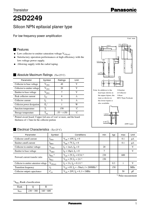
- 5±0.5 Note: In addition to the lead type shown in the upper figure, the type as shown in the lower figure is also available. 1:Emitter 2:Collector 3:Base MT2 Type Package
- 2±0.1 0.65 max.
- 1 0.45+ - 0.05 Printed circuit board: Copper foil area of thickness of 1.7mm for the collector portion or more, and the board
- 5±0.1 (HW type) s Electrical Characteristics Parameter Collector cutoff current Emitter cutoff current Collector to emitter voltage Emitter to base voltage Forward current transfer ratio Collector to emitter saturation voltage Transition frequency Collector output capacitance (Ta=25˚C) Symbol ICBO IEBO VCEO VEBO hFE1 hFE2 VCE(sat) fT Cob
- 1 Conditions VCB = 10V, IE = 0 VEB = 7V, IC = 0 IC = 1mA, IB = 0 IE = 10µA, IC = 0 VCE = 2V, IC = 0.5A*2 VCE = 2V, IC = 2A*2 IC = 3A, IB = 0.1A*2 VCB = 6V, IE = -50mA, f = 200MHz*2 VCB = 20V, IE = 0, f = 1MHz min typ max 0.1 0.1