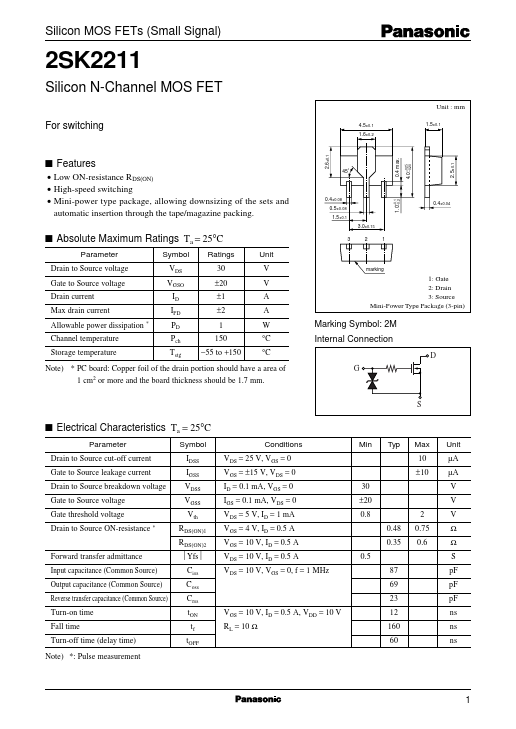
Overview: Silicon MOS FETs (Small Signal) 2SK2211
Silicon N-Channel MOS FET
Unit : mm For switching
2.6±0.1 4.5±0.1 1.6±0.2 1.5±0.1 • Low ON-resistance RDS(ON) • High-speed switching • Mini-power type package, allowing downsizing of the sets and automatic insertion through the tape/magazine packing. 45˚ 1.0–0.2 +0.1 0.4±0.08 0.5±0.08 1.5±0.1 3.0±0.15 4.0+0.25 –0.20 0.4±0.04 s Absolute Maximum Ratings Ta = 25°C
Parameter Drain to Source voltage Gate to Source voltage Drain current Max drain current Allowable power dissipation Channel temperature Storage temperature
* 3 2 1 Symbol VDS VGSO ID IPD PD Pch Tstg Ratings 30 ±20 ±1 ±2 1 150 −55 to +150 Unit V V A A W °C °C
marking 1: Gate 2: Drain 3: Source Mini-Power Type Package (3-pin) Marking Symbol: 2M Internal Connection
D G Note) * PC board: Copper foil of the drain portion should have a area of 1 cm2 or more and the board thickness should be 1.7 mm. S s Electrical Characteristics Ta = 25°C
Parameter Drain to Source cut-off current Gate to Source leakage current Drain to Source breakdown voltage Gate to Source voltage Gate threshold voltage Drain to Source ON-resistance * Symbol IDSS IGSS VDSS VGSS Vth RDS(ON)1 RDS(ON)2 Forward transfer admittance Input capacitance (Common Source) Output capacitance (Common Source) Reverse transfer capacitance (Common Source) Turn-on time Fall time Turn-off time (delay time) Note) *: Pulse measurement Yfs Ciss Coss Crss tON tf tOFF VGS = 10 V, ID = 0.5 A, VDD = 10 V RL = 10 Ω Conditions VDS = 25 V, VGS = 0 VGS = ±15 V, VDS = 0 ID = 0.1 mA, VGS = 0 IGS = 0.1 mA, VDS = 0 VDS = 5 V, ID = 1 mA VGS = 4 V, ID = 0.5 A VGS = 10 V, ID = 0.5 A VDS = 10 V, ID = 0.5 A VDS = 10 V, VGS = 0, f = 1 MHz 0.5 87 69 23 12 160 60 30 ±20 0.8 0.48 0.35 2 0.75 0.6 Min Typ Max 10 ±10 Unit µA µA V V V Ω Ω S pF pF pF ns ns ns 2.5±0.