2SK3032
Overview
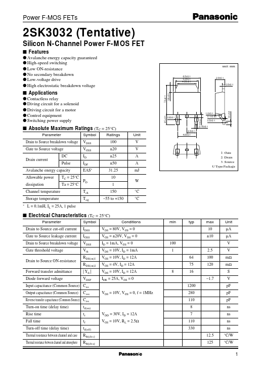
- 3±0.1 1.8±0.1 unit: mm
- 5±0.1 5.3±0.1 4.35±0.1 2.3±0.1 0.5±0.1 s Applications
- 5±0.1
- 93±0.1
- 0±0.1 0.1±0.05 0.5±0.1 s Absolute Maximum Ratings (TC = 25°C) Parameter Drain to Source breakdown voltage Gate to Source voltage Drain current DC Pulse Symbol VDSS VGSS ID IDP EAS* PD Tch Tstg Ratings 100 ±20 ±25 ±50 31.25 10 1 150 -55 to +150 Unit V V A A mJ W °C °C 1 2
- 75±0.1 2.3±0.1 4.6±0.1 3 1: Gate 2: Drain 3: Source U Type Package Avalanche energy capacity Allowable power dissipation Channel temperature Storage temperature * TC = 25°C Ta = 25°C L = 0.1mH, IL = 25A, 1 pulse s Electrical Characteristics (TC = 25°C) Parameter Drain to Source cut-off current Gate to Source leakage current Drain to Source breakdown voltage Gate threshold voltage Drain to Source ON-resistance Forward transfer admittance Diode forward voltage Symbol IDSS IGSS VDSS Vth RDS(on)1 RDS(on)2 | Yfs | VDSF Coss td(on) tr tf td(off) Rth(ch-c) Rth(ch-a) VDD = 30V, ID = 12A VGS = 10V, RL = 2.5Ω Conditions VDS = 80V, VGS = 0 VGS = ±20V, VDS = 0 ID = 1mA, VGS = 0 VDS = 10V, ID = 1mA VGS = 10V, ID = 12A VGS = 4V, ID = 12A VDS = 10V, ID = 12A IDR = 25A, VGS = 0 1200 VDS = 10V, VGS = 0, f = 1MHz 280 110 8 7 110 330 12.5 125 8 100 1 64 75 16 -1.7 2.5 100 120 min typ max 10 ±10 Unit µA µA V V mΩ mΩ S V pF pF pF ns ns ns ns °C/W °C/W Input capacitance (Common Source) Ciss Output capacitance (Common Source) Reverse transfer capacitance (Common Source) Crss Turn-on time (delay time) Rise time Fall time Turn-off time (delay time) Thermal resistance between channel and case Th