AN9E
Overview
- High design flexibility
- Easy circuit constant design because of setting resistance or capacitance to an arbitrary value.
- Free setting of contacts between a substrate and GND wiring prevents from operation error to be caused by floating of substrate potential.
- Usable for multi power source because a resistor island potential can be set for each unit.
- Builds in a lateral type PNP transistor of high reverse breakdown voltage between base and emitter, or a collector wall type NPN transistor of excellent saturation characteristics. (AN9DA00, AN9DB00, AN9DF00)
- Short development period
- Due to a full automatic layout design, a sample is available in one month from a completion of a circuit diagram.
- Applicable to a small quantity production item
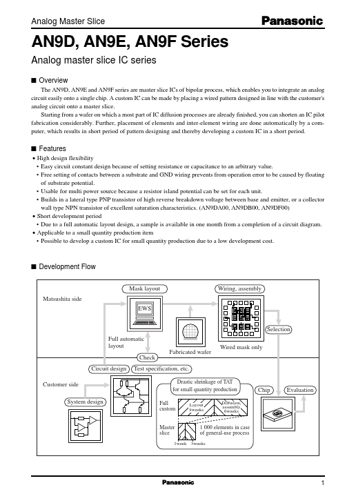
- Possible to develop a custom IC for small quantity production due to a low development cost. s Development Flow Mask layout Matsushita side EWS Selection Full automatic layout Check Circuit design Customer side System design Fabricated wafer Wired mask only Wiring, assembly Test specification, etc. Drastic shrinkage of TAT for small quantity production Full custom Master slice Layout 8weeks Diffusion, assembly 6weeks Chip Evaluation 1 000 elements in case of general-use process 1week 3weeks