Datasheet4U Logo Datasheet4U.com

GN01096B Datasheet GaAs MMIC

Manufacturer: Panasonic

Overview

GaAs MMIC GN01096B GaAs IC (with built-in ferroelectric)
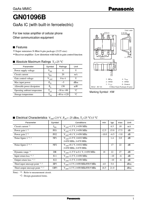
 Unit: mm 1.25±0.1 R0.2 1 0.65 2 0.65 3 0.425 • Super miniature S-Mini 6-pin package (2125 size) • Receiver amplifier : Low distortion with built-in gain control function 2.0±0.1 6 - 0° to 10° s Absolute Maximum Ratings Ta=25 °C Parameter Power supply voltage Circuit current Gate control voltage Max input power Allowable power dissipation Operating ambient temperature Storage temperature Symbol VDD IDD VAGC PIN PD Topr Tstg Ratings 8 20 0 to 4 −5 150 −30 to +90 −40 to +120 Unit 0 to 0.1 V mA V dBm mW °C °C EIAJ : SC-88 1 : RFIN 4 : VDD 2 : GND 5 : GND 3 : VAGC 6 : Source S Mini Type Package (6-pin) Marking Symbol : KW s Electrical Characteristics VDD=2.9 V, PIN=−25 dBm, Ta=25 °C±3 °C Parameter Circuit current *1 Symbol IDD PG1 PG2 NF1 NF2 DR S11 S22 *1, 2 *1, 2 Conditions VAGC=1.5 V, f=850 MHz VAGC=1.5 V, f=850 MHz VAGC=0.1 V, f=850 MHz VAGC=1.5 V, f=832 MHz f=850 MHz, f=870 MHz VAGC=0.1 V, f=832 MHz f=850 MHz, f=870 MHz VAGC=1.5 V to 0.1 V, f=850 MHz VAGC=1.5 V, f=850 MHz VAGC=1.5 V, f=850 MHz VAGC=1.5 V, f=850 MHz/850.9 MHz VAGC=1.5 V, f=850 MHz/850.9 MHz min typ 6.5 0.7±0.1 0.9±0.1 0.2 max 10 17.5 −3.0 2.0 22 27 −6 −6 Unit mA dB dB dB dB dB dB dB dBm dBm Power gain 1 *1 Power gain 2 *1 12.5 −10.0 15.0 −6.5 1.4 17 Noise figure 1 *1, 2 Noise figure 2 *1, 2 Dynamic range *1 Input return loss *1, 2 18 22 −10 −10 Output return loss *1, 2 Third input intersept point IIP3 OIP3 4.0 16.5 5.8 21.0 Third output intersept point Note) *1 : Refer to measurement circuit.

*2 : Design-guaranteed items.

0.2±0.

Key Features

  • 2.1±0.1 0.1 For low noise amplifier of cellular phone Other communication equipment 0.2±0.05 0.12 +0.05.
  • 0.02 4 6 5 0.425 1 GN01096B s Measurement Circuit 1000 pF GaAs MMIC 1.4 pF 39 nH 100 pF RFOUT 0.5 pF 82 Ω 22 nH 100 pF 6 5 4 3 1 2 33 pF RFIN 27 nH 5.1 kΩ VAGC 12 pF 10 nF 2.