MN3867S Overview
Key Features
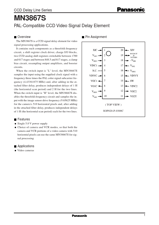
- VBB VSS2 VDD2 VINVY SW VINC2 VGC2 VO2Y
| Part | MN3867S |
|---|---|
| Description | PAL-Compatible CCD Video Signal Delay Element |
| Manufacturer | Panasonic |
| Size | 64.74 KB |
| Part Number | Manufacturer | Description |
|---|---|---|
| MN3860 | Integrated Circuit Systems | 12-bit D/A Converter with Input Register |