0.05
s Absolute Maximum Ratings Ta = 25°C
Parameter Reverse voltage (DC) Forward current (DC) Power dissipation Junction temperature Storage temperature Symbol VR IF PD Tj Tstg Rating 60 100 150 150.
55 to +150 Unit
0.01±0.01
V mA mW °C °C
1: Anode 2: Cathode SSMini2-F1 Package
Marking Symbol: 2P
s Electrical Characteristics Ta = 25°C ± 3°C
Parameter Reverse current (DC) Forward voltage (DC) Terminal capacitance Forward.
The following content is an automatically extracted verbatim text
from the original manufacturer datasheet and is provided for reference purposes only.
View original datasheet text
PIN diodes
www.DataSheet4U.com
MA2SP01
Silicon epitaxial planar type
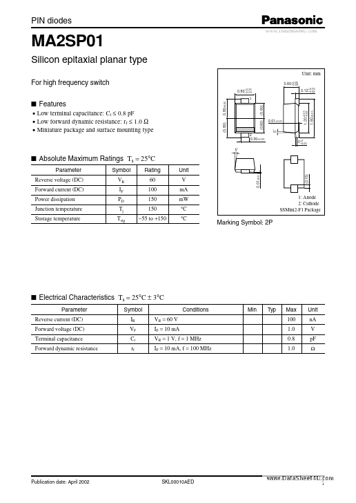
Unit: mm
For high frequency switch
0.80+0.05 –0.03
0.80±0.05
0.60+0.05 –0.03 0.12+0.05 –0.02
• Low terminal capacitance: Ct ≤ 0.8 pF • Low forward dynamic resistance: rf ≤ 1.0 Ω • Miniature package and surface mounting type
(0.60)
s Features
1
(0.80)
(0.60)
0.01±0.01
5˚
2 0.30±0.05 5˚
0+0 –0.05
s Absolute Maximum Ratings Ta = 25°C
Parameter Reverse voltage (DC) Forward current (DC) Power dissipation Junction temperature Storage temperature Symbol VR IF PD Tj Tstg Rating 60 100 150 150 −55 to +150 Unit
0.01±0.