Overview: Schottky Barrier Diodes (SBD)
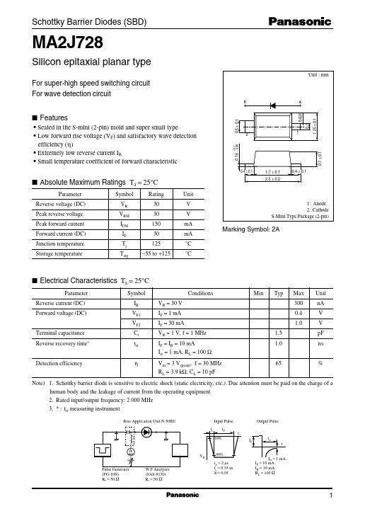
 MA2J728
Silicon epitaxial planar type
Unit : mm For super-high speed switching circuit For wave detection circuit
K A
0.625 0.4 ± 0.1 1.7 ± 0.1 2.5 ± 0.2 0.4 ± 0.1 I Absolute Maximum Ratings Ta = 25°C
Parameter Reverse voltage (DC) Peak reverse voltage Peak forward current Forward current (DC) Junction temperature Storage temperature Symbol VR VRM IFM IF Tj Tstg Rating 30 30 150 30 125 −55 to +125 Unit V V mA mA °C °C 1 : Anode 2 : Cathode S-Mini Type Package (2-pin) Marking Symbol: 2A I Electrical Characteristics Ta = 25°C
Parameter Reverse current (DC) Forward voltage (DC) Symbol IR VF1 VF2 Terminal capacitance Reverse recovery time* Ct trr η VR = 30 V IF = 1 mA IF = 30 mA VR = 1 V, f = 1 MHz IF = IR = 10 mA Irr = 1 mA, RL = 100 Ω Vin = 3 V(peak), f = 30 MHz RL = 3.9 kΩ, CL = 10 pF 1.5 1.0 Conditions Min Typ Max 300 0.4 1.0 Unit nA V V pF ns Detection efficiency 65 Note) 1. Schottky barrier diode is sensitive to electric shock (static electricity, etc.). Due attention must be paid on the charge of a human body and the leakage of current from the operating equipment 2. Rated input/output frequency: 2 000 MHz 3. * : trr measuring instrument
Bias Applicaiton Unit N-50BU tr 10% Input Pulse tp t IF trr t Irr = 1 mA IF = 10 mA IR = 10 mA RL = 100 Ω Output Pulse A
VR Pulse Generator (PG-10N) Rs = 50 Ω W.F.Analyzer (SAS-8130) Ri = 50 Ω 90% tp = 2 µs tr = 0.35 ns δ = 0.05 0.7 ± 0.1 • Sealed in the S-mini (2-pin) mold and super small type • Low forward rise voltage (VF) and satisfactory wave detection efficiency (η) • Extremely low reverse current IR • Small temperature coefficient of forward characteristic 2
0.16 − 0.06
+ 0.1 1 1.25 ± 0.1 0.5 ± 0.