PI6C3Q993
PI6C3Q993 is 3.3V Programmable Skew PLL Clock Driver manufactured by Pericom Semiconductor.
- Part of the PI6C3Q991 comparator family.
- Part of the PI6C3Q991 comparator family.
Features
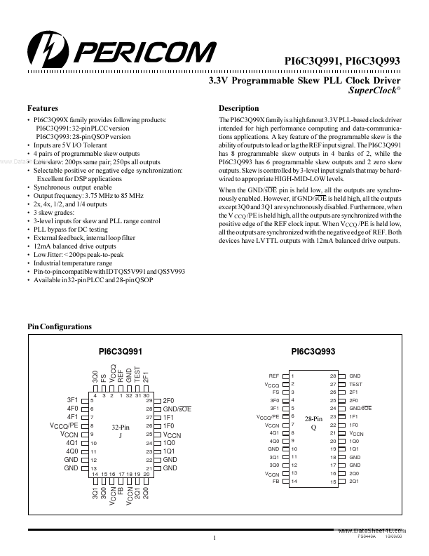
PI6C3Q99X family provides following products: PI6C3Q991: 32-pin PLCC version PI6C3Q993: 28-pin QSOP version Inputs are 5V I/O Tolerant 4 pairs of programmable skew outputs .. Low skew: 200ps same pair; 250ps all outputs Selectable positive or negative edge synchronization: Excellent for DSP applications Synchronous output enable Output frequency: 3.75 MHz to 85 MHz 2x, 4x, 1/2, and 1/4 outputs 3 skew grades: 3-level inputs for skew and PLL range control PLL bypass for DC testing External feedback, internal loop filter 12m A balanced drive outputs Low Jitter: < 200ps peak-to-peak Industrial temperature range Pin-to-pin patible with IDT QS5V991 and QS5V993 Available in 32-pin PLCC and 28-pin QSOP
Description
The PI6C3Q99X family is a high fanout 3.3V PLL-based clock driver intended for high performance puting and data-munications applications. A key feature of the programmable skew is the ability of outputs to lead or lag the REF input signal. The PI6C3Q991 has 8 programmable skew outputs in 4 banks of 2, while the PI6C3Q993 has 6 programmable skew outputs and 2 zero skew outputs. Skew is controlled by 3-level input signals that may be hardwired to appropriate HIGH-MID-LOW levels. When the GND/s OE pin is held low, all the outputs are synchronously enabled. However, if GND/s OE is held high, all the outputs except 3Q0 and 3Q1 are synchronously disabled. Furthermore, when the V CCQ /PE is held high, all the outputs are synchronized with the positive edge of the REF clock input. When VCCQ /PE is held low, all the outputs are synchronized with the negative edge of REF. Both devices have LVTTL outputs with 12m A balanced drive outputs.
Pin Configurations PI6C3Q991
3Q0 FS VCCQ REF GND TEST 2F1
REF VCCQ FS
1 2 3 4 5 6 7 8 9 10 11 12 13 14 28 27 26 25 24
GND TEST 2F1 2F0 GND/s OE 1F1 1F0 VCCN 1Q0 1Q1 GND GND 2Q0 2Q1
3F1 4F0 4F1 VCCQ/PE VCCN 4Q1 4Q0 GND GND
4 5 6 7 8 9 10 11 12
3 2
1 32 31 30 29 28 27 26 25 24 23...