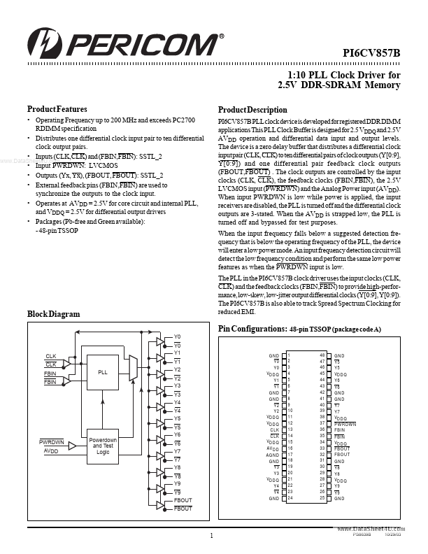
Datasheet4U Logo Datasheet4U.com

PI6CV857B - 1:10 PLL Clock Driver

General Description

PI6CV857B PLL clock device is developed for registered DDR DIMM applications This PLL Clock Buffer is designed for 2.5 VDDQ and 2.5V AVDD operation and differential data input and output levels.

Key Features

  • Operating Frequency up to 200 MHz and exceeds PC2700 RDIMM specification.
  • Distributes one differential clock input pair to ten differential clock output pairs.
  • Inputs (CLK,CLK) and (FBIN,FBIN): SSTL_2 www. DataSheet4U. com.
  • Input PWRDWN: LVCMOS.
  • Outputs (Yx, Yx), (FBOUT, FBOUT): SSTL_2.
  • External feedback pins (FBIN,FBIN) are used to synchronize the outputs to the clock input.
  • Operates at AVDD = 2.5V for core circuit and internal PLL.

📥 Download Datasheet

Full PDF Text Transcription (Reference)

The following content is an automatically extracted verbatim text from the original manufacturer datasheet and is provided for reference purposes only.

View original datasheet text
12345678901234567890123456789012123456789012345678901234567890121234567890123456789012345678901212345678901234567890123456789012123456789012 PI6CV857B 1:10 PLL Clock Driver for 2.5V DDR-SDRAM Memory Product Features • Operating Frequency up to 200 MHz and exceeds PC2700 RDIMM specification • Distributes one differential clock input pair to ten differential clock output pairs. • Inputs (CLK,CLK) and (FBIN,FBIN): SSTL_2 www.DataSheet4U.com • Input PWRDWN: LVCMOS • Outputs (Yx, Yx), (FBOUT, FBOUT): SSTL_2 • External feedback pins (FBIN,FBIN) are used to synchronize the outputs to the clock input. • Operates at AVDD = 2.5V for core circuit and internal PLL, and VDDQ = 2.