PI74SSTVF16859
PI74SSTVF16859 is 13-Bit to 26-Bit Registered Buffer manufactured by Pericom Semiconductor.
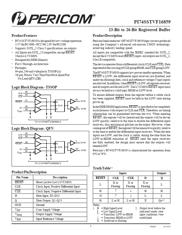
Features
- PI74 SSTVF16859 is designed for low-voltage operation, 2.5V for PC1600 ~ PC2700; 2.6V for PC3200
- Supports SSTL_2 Class I specifications on outputs
- All Inputs are SSTL_2 patible, except RESET which is LVCMOS.
- Designed for DDR Memory
- Flow-Through Architecture
- Packages: 64-pin, 240-mil wide plastic TSSOP (A) 56-pin, Plastic Very Thin Fine Pitch Quad Flat No Lead QFN (ZB)
Product Description
Peri Semiconductor’s PI74SSTVF16859 logic circuit is produced using the pany’s advanced sub-micron CMOS technology, achieving industry leading speed. All inputs are patible with the JEDEC standard for SSTL_2, except the LVCMOS reset (RESET) input. All outputs are SSTL_2, Class II patible. The device operates from a differential clock (CLK and CLK). Data registered at the crossing of CLK going HIGH, and CLK going LOW. The PI74SSTVF16859 supports low-power standby operation. When RESET is LOW, the differential input receivers are disabled, and undriven (floating) data, clock and reference voltage (VREF) inputs are allowed. In addition, when RESET is LOW, all registers are reset, and all outputs are forced LOW. The LVCMOS RESET input must always be held at a valid logic HIGH or LOW level. To ensure defined outputs from the register before a stable clock has been supplied, RESET must be held in the LOW state during power up. In the DDR DIMM application, RESET is specified to be pletely asynchronous with respect to CLK and CLK. Therefore, no timing relationship can be guaranteed between the two. When entering RESET, the register will be cleared and the outputs will be driven LOW quickly, relative to the time to disable the differential input receivers, thus ensuring no glitches on the output. However, when ing out of RESET, the register will bee active quickly, relative to the time to enable the differential input receivers. When the data inputs are LOW, and the clock is stable, during the time from the LOW-to-HIGH transition of RESET until the input receivers are...