PI90LVB044
PI90LVB044 is LVDS Dual 2x2 Crosspoint/Repeater Switch manufactured by Pericom Semiconductor.
- Part of the PI90LV044 comparator family.
- Part of the PI90LV044 comparator family.
Features
- Dual 2x2 Crosspoint/Repeater Switch
- Meets or Exceeds the Requirements of ANSI TIA/EIA-644-1995
- Designed for Signaling Rates up to 650 Mbit/s (325Mhz)
- Operates from a single 3.3V Supply:
- 40°C to 85°C
- Low-Voltage Differential Signaling with Output Voltages of ±350m V into:
- 100Ω load (PI90LV044)
- 50Ω load Bus LVDS Signaling (PI90LVB044)
- Accepts ±350m V differential inputs
- Wide mon mode input range: 0.2V to 2.7V
- Output drivers are high impedance when disabled or when VCC ≤ 1.5V
- Inputs are open, short, and terminated fail safe
- Propagation Delay Time: 3.5ns
- ESD protection is 10k V on bus pins
- Bus Pins are High Impedance when disabled or with VCC less than 1.5V
- TTL Inputs are 5V Tolerant
- Power Dissipation at 400 Mbit/s of 250m W
- Packaging (Pb-free & Green available):
- 28-pin QSOP (Q)
- 28-pin TSSOP (L)
Description
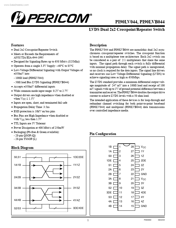
The PI90LV044 and PI90LVB044 are monolithic dual 2x2 asynchronous crosspoint/repeater switches. The crosspoint function is based on a multiplexer tree architecture. Each 2x2 switch can be considered as a pair of 2:1 multiplexers that share the same inputs. The signal path through each switch is fully differential with minimal propagation delay. The signal path is unregistered, so no clock is required for the data inputs. The signal line drivers and receivers use Low Voltage Differential Signaling (LVDS) to achieve signaling rates as high as 650Mbps. The LVDS standard provides a minimum differential output voltage magnitude of 247 m V into a 100Ω load and receipt of 100 m V signals with up to 1V of ground potential difference between a transmitter and receiver. The PI90LVB044 doubles the output drive current to achieve LVDS levels with a 50 ohm load. The intended application of these devices is for loop-through and redundant channel switching for both point-to-point baseband (PI90LV044) and multipoint (PI90LVB044) data transmissions over controlled impedance media.
Pin Configuration
Block Diagram
S0,S1 1A/1B 1DE/2DE...