PDM6T20V3
PDM6T20V3 is N- & P-Channel MOSFET manufactured by Prisemi.
PDM6T20V3 N-Channel and P-Channel MOSFET
Description
The enhancement mode MOS is extremely high density cell and low on-resistance.
MOSFET Product Summary
VDS(V)
RDS(on)(Ω)
N-Channel 20
0.043@ VGS=4.5V
P-Channel -20
0.08@ VGS=-4.5V
ID(A) 3
-2.8
N-Channel
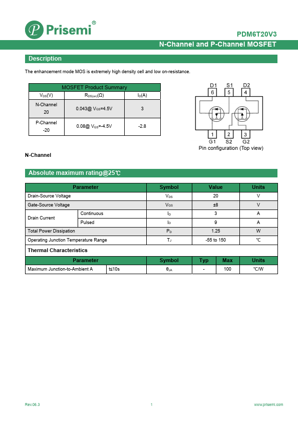
Pin configuration (Top...