PPM6N20V5 Overview
Description
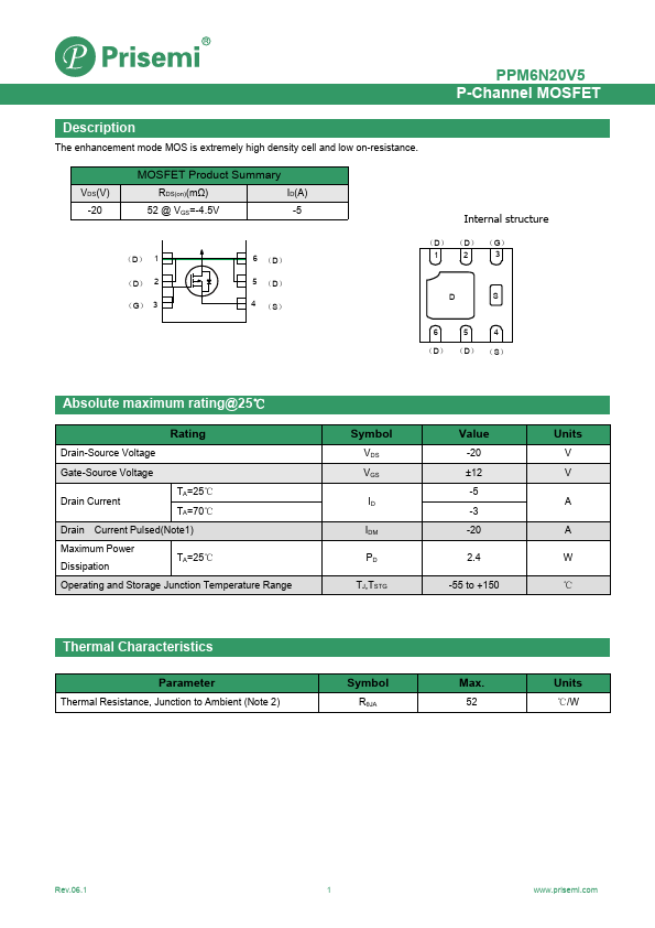
The enhancement mode MOS is extremely high density cell and low on-resistance. VDS(V) -20 MOSFET Product Summary RDS(on)(mΩ) ID(A) 52 @ VGS=-4.5V -5 (D) 1 (D) 2 (G) 3 6 (D) 5 (D) 4 (S) Internal structure (D) (D) (G) 12 3 DS 65 4 (D) (D) (S) Absolute maximum rating@25℃ Rating Drain-Source Voltage Gate-Source Voltage Drain Current TA=25℃ TA=70℃ Drain Current Pulsed(Note1) Maximum Power Dissipation TA=25℃ Operating and Storage Junction Temperature Range Symbol VDS VGS ID IDM PD TJ,TSTG Value -20 ±12 -5 -3 -20 2.4 -55 to +150 Units V V A A W ℃ Parameter Symbol RθJA Max.