PPM6N30V4
Description
The enhancement mode MOS is extremely high density cell and low on-resistance.
PPM6N30V4 P-Channel MOSFET
VDS(V) -30
MOSFET Product Summary
RDS(on)(Ω)
ID(A)
0.053 @ VGS=-10V -4.2
0.065@ VGS=-4.5V
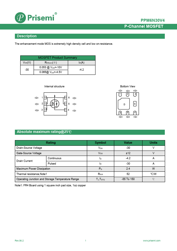
Internal structure
(D) 1 (D) 2 (G) 3
6 (D) 5 (D) 4 (S)
Bottom View
(D) (D) (G)
(D) (D) (S)
Absolute maximum rating@25℃
Rating
Drain-Source Voltage
Gate-Source Voltage
Drain Current
Continuous Pulsed
Maximum Power Dissipation
Thermal resistance,Note1
Operating Junction and Storage Temperature Range
Note1: FR4 Board using 1 square inch pad size, 1oz copper
Symbol
VDS VGS ID ID PD RθJA TJ,TSTG
Value
-30 ±12 -4.2 -30 2.4 52 -55 To 150
Units
V V A A W ℃/W ℃
Rev.06.2
.prisemi.
P-Channel MOSFET
Electrical characteristics per line@25℃( unless otherwise specified)
Parameter
Drain-Source Breakdown Voltage Zero Gate Voltage Drain...