PPM6N30V9
Description
The enhancement mode MOS is extremely high density cell and low on-resistance.
PPM6N30V9 P-Channel MOSFET
VDS(V) -30
MOSFET Product Summary
RDS(on)(mΩ)
ID(A)
21 @ VGS=-4.5V
-9
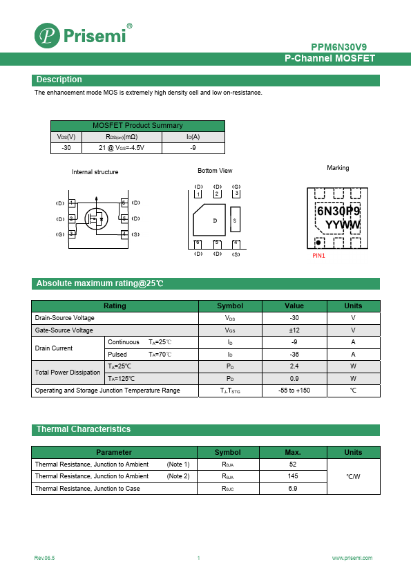
Internal structure
(D) 1 (D) 2 (G) 3
6 (D) 5 (D) 4 (S)
Bottom View
(D) (D) (G)
(D) (D) (S)
Absolute maximum rating@25℃
Rating
Drain-Source Voltage
Gate-Source Voltage
Drain Current
Continuous Pulsed
TA=25℃ TA=70℃
TA=25℃ Total Power Dissipation
TA=125℃
Operating and Storage Junction Temperature Range
Symbol
VDS VGS ID ID PD PD TJ,TSTG
Marking
Value
-30 ±12 -9 -36 2.4 0.9 -55 to +150
Units
V V A A W W ℃
Thermal Characteristics
Parameter
Thermal Resistance, Junction to Ambient Thermal Resistance, Junction to Ambient Thermal Resistance, Junction to Case
(Note 1) (Note 2)
Symbol
RθJA RθJA...