PulseCore ASM2P5T905A
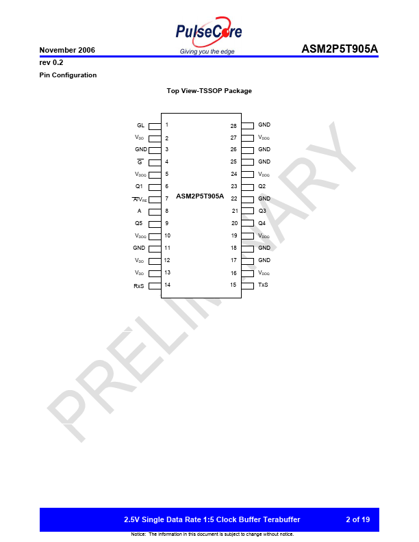
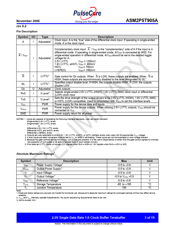
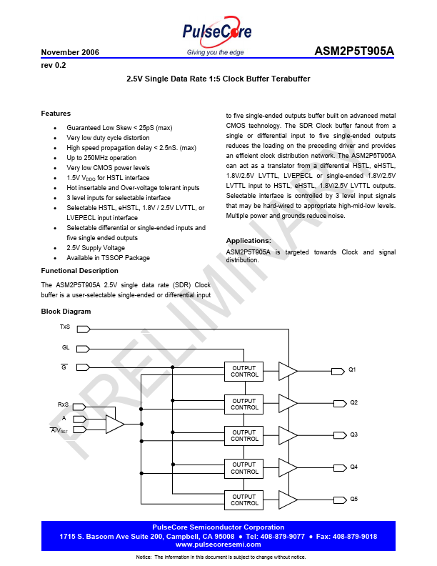
The ASM2P5T905A 2.5V single data rate (SDR) Clock buffer is a user-selectable single-ended or differential input Block Diagram TxS to five single-ended outputs buffer built on advanced metal CMOS technology. The SDR Clock buffer fanout from a single or differential input to five single-ended outputs reduces the loading on the preceding driver and provides an efficient clock distribution network. The ASM2P5T905A can act as a translator from a differential HSTL, eHSTL, 1.8V/2.5V LVTTL, LVEPECL or single-ended 1.8V/2.5V LVTTL input to HSTL, eHSTL, 1.8V/2.5V LVTTL outputs.| Part No. | ASM2P5T905A |
|---|---|
| Datasheet | ASM2P5T905A Download |
| Manufacturer | PulseCore |
| Description | 2.5V Single Data Rate 1:5 Clock Buffer Terabuffer |
| Buy | Stock & Price |
FEATURES
● Guaranteed Low Skew < 25pS (max)● Very low duty cycle distortion
● High speed propagation delay < 2.5nS. (max)
● Up to 250MHz operation
● Very low CMOS power levels
● 1.5V VDDQ for HSTL interface
● Hot insertable and Over-voltage tolerant inputs
● 3 level inputs for selectable interface
● Selectable HSTL, eHSTL, 1.8V / 2.5V LVTTL, or LVEPECL input interface
● Selectable differential or single-ended inputs and five single ended outputs
● 2.5V Supply Voltage
● Available in TSSOP Package Functional
DESCRIPTION
Selectable interface is controlled by 3 level input signals that may be hard-wired to appropriate high-mid-low levels. Multiple power and grounds reduce noise.APPLICATIONS
: ASM2P5T905A is targeted towards Clock and signal distribution. GL G OUTPUT Q1 CONTROL RxS A A/VREF OUTPUT CONTROL OUTPUT CONTROL Q2 Q3 OUTPUT CONTROL Q4 OUTPUT CONTROL Q5 PulseCore Semiconductor Corporation 1715 S. Bascom Ave Suite 200, Campbell, CA 95008● Tel: 408-879-9077
● Fax: 408-879-9018 Notice: The information in this document is subject to change without notice.