RCR1525SI Overview
Key Features
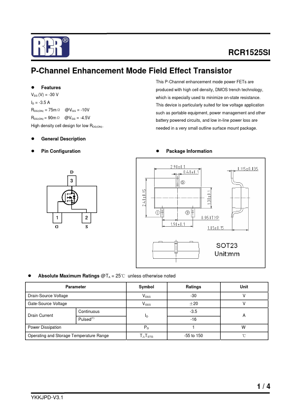
- Package Information D 3 12 GS
- Parameter Symbol Test Conditions Min Typ OFF CHARACTERISTICS Drain-Source Breakdown Voltage V(BR)DSS VGS = 0 V, ID = -250 µA
- 30 -- Zero Gate Voltage Drain Current IDSS VDS = -30 V, VGS = 0 V -- -- Gate
- Body Leakage, Forward IGSSF VGS = +20 V, VDS = 0 V
- Body Leakage, Reverse IGSSR VGS = -20 V, VDS = 0 V ON CHARACTERISTICS (2)
- Gate Threshold Voltage VGS (th) VDS = VGS, ID = -250 µA
- 1 -1.4 Static Drain-Source On-Resistance RDS(ON) VGS = -4.5 V, ID = -3 A VGS = -10 V, ID = -4.1 A
- 680 -- 72 -- 58 Turn-On Delay Time Turn-On Rise Time Turn-Off Delay Time Turn-Off Fall Time td(on) tr td(off) tf VDD = -6 V, RL = 6Ω,ID = -1