SIW1721B
SIW1721B is BLUETOOTH RADIO MODEM manufactured by RF Micro Devices.
Features
- Integrated RF transceiver and modem for Bluetooth wireless technology.
- Manufactured using low-power 0.18-micron CMOS process technology.
- Digital baseband interface connects directly to an integrated Bluetooth controller.
- Direct conversion RF architecture improves receiver-blocking performance.
- Low out-of-band spurious emissions minimize interference with mobile phone operations.
- Hardware AGC dynamically adjusts receiver performance in changing environments.
- 50 Ω RF I/O does not need additional external impedance matching ponents.
- On-chip voltage regulation simplifies system design.
- -88 d Bm receiver sensitivity and +2 d Bm transmitter power typical performance specifications.
- Bluetooth Specification V2.0 qualified. plies with Bluetooth specifications V1.1, V1.2 and V2.0.
Reference Clock Ext Power
BLUETOOTH® RADIO MODEM
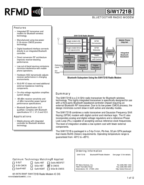
Si W1721B Radio Modem Single-ended LNA ADC and Downconverter Single-ended Driver DAC and Upconverter GFSK Demodulator GFSK Modulator Radio Programming and Control SPI CLK Circuit Analog Regulator Digital Regulator Mobile Phone Chip Set
Modem I/F & Data
Reference PLL
Modem Clock Generator
Integrated Bluetooth Baseband
Bluetooth Subsystem Using the Si W1721B Radio Modem
Summary
The Si W1721B is a 2.4-GHz radio transceiver for Bluetooth wireless technology. This highly integrated transceiver is specifically designed for use with a third party Bluetooth baseband controller chipset requiring an external Bluetooth RF transceiver. Due to its low power CMOS process, the design minimizes current draw in both active and standby modes. The Si W1721B bines a radio transceiver and Gaussian Frequency Shift Keying (GFSK) modem with digital control and interface logic. The IC also incorporates analog and digital voltage regulators and a reference Phase Lock Loop (PLL) capable of accepting various reference clock frequencies. The level of integration enables a low system cost with fewer external ponents. The Si W1721B is packaged in a...