Datasheet Summary
General Purpose CMOS Logic IC
Single 2-Input NAND Gate
General Description
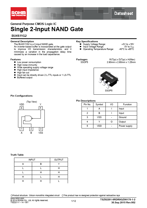
The BU4S11G2 is a 2-input NAND gate. An inverter-based buffer is incorporated at the gate output to improve I/O transmission characteristics, and it minimizes a variation in the propagation delay time caused by an increase in the load capacitance.
Key Specifications
- Supply Voltage Range:
- Input Voltage Range:
- Operating Temperature Range:
+3V to +16V 0V to VDD
-40°C to +85°C
Features
- Low power consumption
- High noise immunity
- Wide operating supply voltage range
- High input impedance
- High fan out
- Input can be directly driven 2 L-TTL inputs or 1 LS-TTL
- Buffered output
Packages...