Datasheet Summary
General Purpose CMOS Logic IC
Single Schmitt Trigger Inverter Gate
General Description
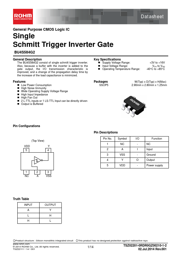
The BU4S584G2 consist of single schmitt trigger inverter. Also, because a buffer with the inverter is added to the gate output, the I/O transmission characteristic is improved, and a change of the propagation delay time by the increase of the load capacitance is minimized.
Key Specifications
- Supply Voltage Range:
- Input Voltage Range:
- Operating Temperature Range:
+3V to +16V VSS to VDD
-40°C to +85°C
Features
- Low Power Consumption
- High Noise Immunity
- Wide Operating Supply Voltage Range
- High Input Impedance
- High Fan Out
- 2 L-TTL inputs or 1 LS-TTL Input can be...