Datasheet Summary
Standard ICs
Single 2-input NAND gate
The BU4S11 is a dual-input positive logic NAND gate. This is an ultra-pact logic IC with one circuit of the BU4011B built into an SMP package. Features
- 1) Low current dissipation. 2) Super-mini mold package designed for surface mounting.
3) Wide range of operating power supply voltage. 4) Capable of driving two L-TTL inputs and one LS-TTL input directly
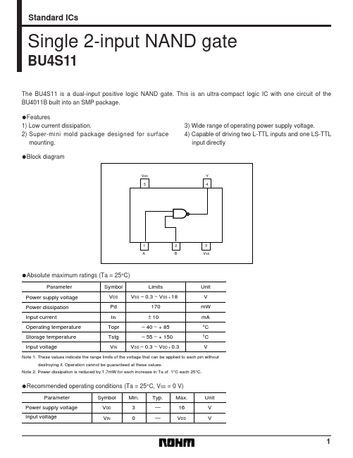
- Block diagram
VDD 5 Y 4
1 A
2 B
3 VSS
-...