HAT2218R
Features
- -
- - Low on-resistance Capable of 4.5 V gate drive High density mounting Built-in Schottky Barrier Diode
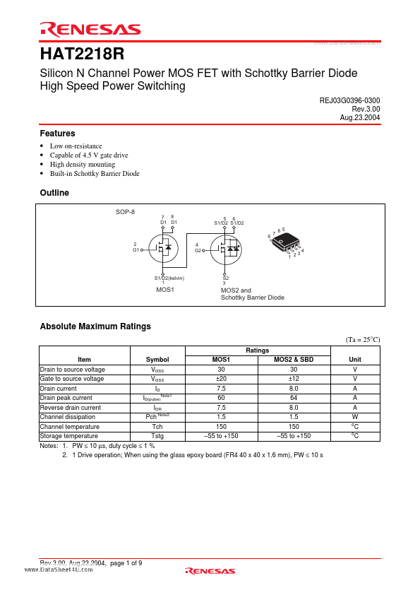
Outline
SOP-8
7 8 D1 D1 5 6 S1/D2 S1/D2 8 2 G1 4 G2 5 7 6
3 1 2
S1/D2(kelvin) 1
S2 3
MOS1
MOS2 and Schottky Barrier Diode
Absolute Maximum Ratings
(Ta = 25°C)
Ratings Item Drain to source voltage Gate to source voltage Drain current Drain peak current Reverse drain current Symbol VDSS VGSS ID ID(pulse)Note1 IDR MOS1 30 ±20 7.5 60 7.5 MOS2 & SBD 30 ±12 8.0 64 8.0 Unit V V A A A W
Channel dissipation Pch Note2 1.5 1.5 Channel temperature Tch 150 150 Storage temperature Tstg
- 55 to +150
- 55 to +150 Notes: 1. PW ≤ 10 µs, duty cycle ≤ 1 % 2. 1 Drive operation; When using the glass epoxy board (FR4 40 x 40 x 1.6 mm), PW ≤ 10 s
°C °C
Rev.3.00, Aug.23.2004, page 1 of 9
Electrical Characteristics
- MOS1
..
(Ta = 25°C)
Item Drain to source breakdown voltage Gate to source leak current Zero gate voltage drain current Gate to source cutoff voltage Static...