RQA0009SXAQS
RQA0009SXAQS is Silicon N-Channel MOS FET manufactured by Renesas.
Features
- High Output Power, High Gain, High Efficiency Pout = +37.8 d Bm, Linear Gain = 18 d B, PAE = 65% (VDS = 6 V, f = 520 MHz)
- pact package capable of surface mounting
- Electrostatic Discharge Immunity Test (IEC Standard, 61000-4-2, Level4)
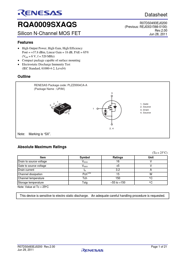
Outline
RENESAS Package code: PLZZ0004CA-A (Package Name : UPAK R )
1. Gate 2. Source 3. Drain 4. Source
2, 4
Note:
Marking is “SX”.
- UPAK is a trademark of Renesas Technology Corp.
Absolute Maximum Ratings
(Ta = 25°C)
Item Drain to source voltage Gate to source voltage Drain current Channel dissipation Channel temperature Storage temperature Note: Value at Tc = 25°C Symbol VDSS VGSS ID Pchnote Tch Tstg Ratings 16 ±5 3.2 15 150
- 55 to +150 Unit V V A W °C °C
This device is sensitive to electro static discharge. An adequate careful handling procedure is requested.
REJ03G1566-0100 Rev.1.00 Jul 04, 2007 Page 1 of 12
Electrical Characteristics
(Ta = 25°C)
Item Zero gate voltage drain current Gate to source leak current Gate to source cutoff voltage Forward Transfer Admittance Input capacitance Output capacitance Reverse transfer capacitance Output Power Power Added Efficiency Output Power Power Added Efficiency Symbol IDSS IGSS VGS(off) |yfs| Ciss Coss Crss Pout PAE Pout PAE Min.
- - 0.15
- -
- -
- -
- -
- - Typ
- - 0.5 3.2 76 40 3.5 37.8 6.0 65 35.2 3.3 60 Max. 15 ±2 0.8
- -
- -
- -
- -
- - Unit µA µA V S p F p F p F d Bm W % d Bm W % Test Conditions VDS = 16 V, VGS = 0 VGS = ±5 V, VDS = 0 VDS = 6 V, ID = 1 m A VDS = 6 V, ID = 1.6 A VGS = 5 V, VDS = 0, f = 1 MHz VDS = 6 V, VGS = 0, f = 1 MHz VDG = 6 V, VGS = 0, f = 1 MHz VDS = 6 V, IDQ = 180 m A f = 520 MHz, Pin = +25 d Bm (316 m W) VDS = 4.8 V, IDQ = 300 m A f = 465 MHz, Pin = +17 d Bm (50 m W)
Main Characteristics
Maximum Channel Power Dissipation Curve Typical Output Characteristics...