ICS672-02 Overview
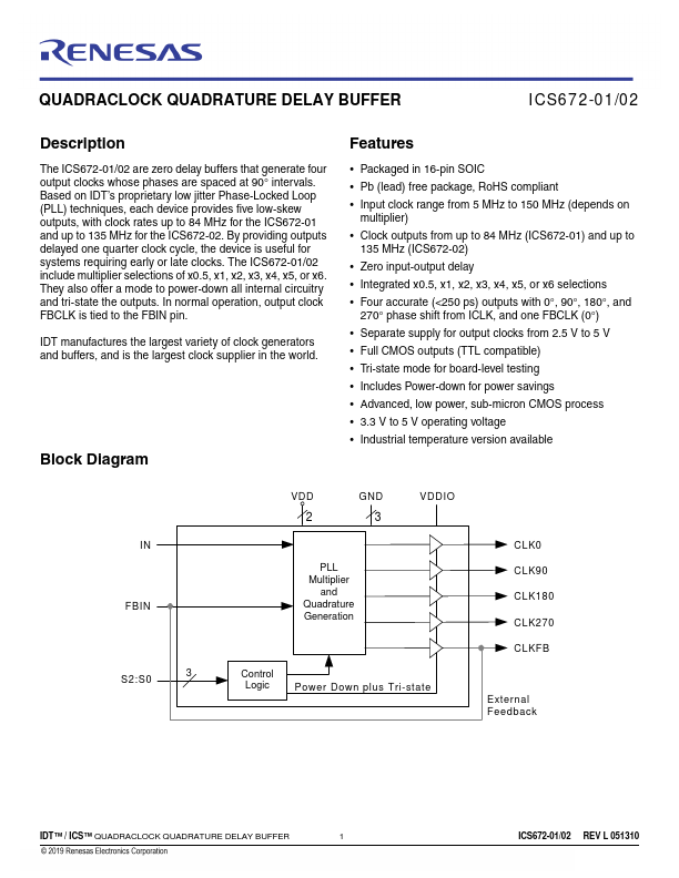
The ICS672-01/02 are zero delay buffers that generate four output clocks whose phases are spaced at 90° intervals. Based on IDT’s proprietary low jitter Phase-Locked Loop (PLL) techniques, each device provides five low-skew outputs, with clock rates up to 84 MHz for the ICS672-01 and up to 135 MHz for the ICS672-02. By providing outputs delayed one quarter clock cycle, the device is useful for systems requiring...
ICS672-02 Key Features
- Packaged in 16-pin SOIC
- Pb (lead) free package, RoHS pliant
- Input clock range from 5 MHz to 150 MHz (depends on
- Zero input-output delay
- Integrated x0.5, x1, x2, x3, x4, x5, or x6 selections
- Four accurate (<250 ps) outputs with 0°, 90°, 180°, and
- Separate supply for output clocks from 2.5 V to 5 V
- Full CMOS outputs (TTL patible)
- Tri-state mode for board-level testing
- Includes Power-down for power savings