ICS8305I-02 Overview
Description
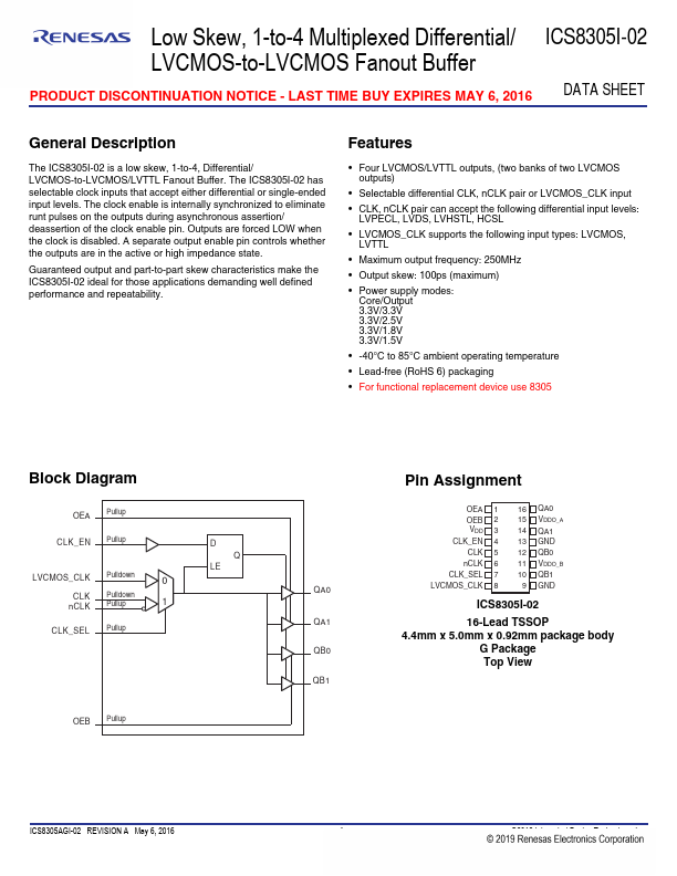
The ICS8305I-02 is a low skew, 1-to-4, Differential/ LVCMOS-to-LVCMOS/LVTTL Fanout Buffer. The ICS8305I-02 has selectable clock inputs that accept either differential or single-ended input levels.
Key Features
- Four LVCMOS/LVTTL outputs, (two banks of two LVCMOS outputs)
- Selectable differential CLK, nCLK pair or LVCMOS_CLK input
- CLK, nCLK pair can accept the following differential input levels: LVPECL, LVDS, LVHSTL, HCSL
- LVCMOS_CLK supports the following input types: LVCMOS, LVTTL
- Maximum output frequency: 250MHz
- Output skew: 100ps (maximum)
- 40°C to 85°C ambient operating temperature
- Lead-free (RoHS
- For functional replacement device use 8305