ICS98UAE877A Overview
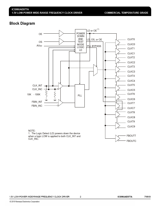
The PLL clock buffer, ICS98UAE877A, is designed for a VDDQ of 1.5V, an AVDD of 1.5V and differential data input and output levels. ICS98UAE877A is a zero delay buffer that distributes a differential clock input pair (CLK_INT, CLK_INC) to ten differential pair of clock outputs (CLKT[0:9], CLKC[0:9]) and one differential pair feedback clock outputs (FB_OUTT, FBOUTC). The clock outputs are controlled by the input...
ICS98UAE877A Key Features
- Low skew, low jitter PLL clock driver
- 1 to 10 differential clock distribution
- Feedback pins for input to output synchronization
- Spread Spectrum tolerant inputs
- Auto PD when input signal is at a certain logic state
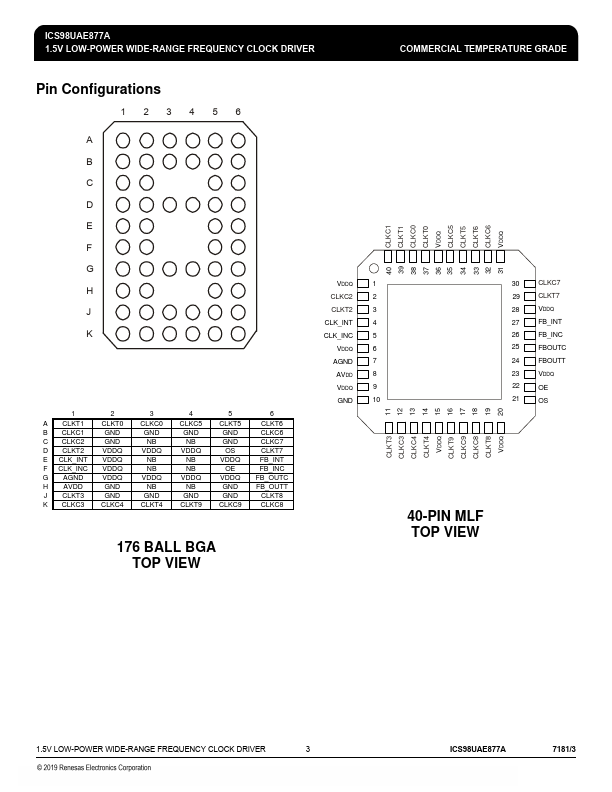
- Available in 52-ball VFBGA and a 40-pin MLF