Datasheet4U Logo Datasheet4U.com

ICSSSTVF16857 - DDR 14-Bit Registered Buffer

Datasheet Summary

Features

  • Differential clock signal.
  • Meets SSTL_2 signal data.
  • Supports SSTL_2 class I & II specifications.
  • Low-voltage operation - Voo = 2.3V to2.7V.
  • 48 pin TSS OP and TVS OP package Truth Table1 Inputs RESET# CLK CLK# L Xor Xor Floating Floating H t J, H t J, H LorH LorH D Xor Floating H L X Q Outputs Q L H L QlZ> Pin Configuration Q1 1 48 D1 Q2 2 47 D2 GND 3 46 GND VDDQ 4 45 VDD QJ 5 44 DJ Q4 6 43 D4 Q5 7 42 D5 ->cc:ooGND VDDQ.

📥 Download Datasheet

Datasheet preview – ICSSSTVF16857

Datasheet Details

Part number ICSSSTVF16857
Manufacturer Renesas
File Size 484.89 KB
Description DDR 14-Bit Registered Buffer
Datasheet download datasheet ICSSSTVF16857 Datasheet
Additional preview pages of the ICSSSTVF16857 datasheet.
Other Datasheets by Renesas

Full PDF Text Transcription

Click to expand full text
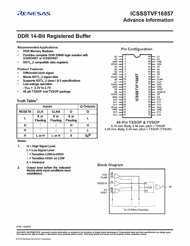
�ENESAS ICSSSTVF16857 Advance Information DDR 14-Bit Registered Buffer Recommended Applications: • DDR Memory Modules • Provides complete DDR DIMM logic solution with ICS93V857 or ICS95V857 • SSTL_2 compatible data registers Product Features: • Differential clock signal • Meets SSTL_2 signal data • Supports SSTL_2 class I & II specifications • Low-voltage operation - Voo = 2.3V to2.7V • 48 pin TSS OP and TVS OP package Truth Table1 Inputs RESET# CLK CLK# L Xor Xor Floating Floating H t J, H t J, H LorH LorH D Xor Floating H L X Q Outputs Q L H L QlZ> Pin Configuration Q1 1 48 D1 Q2 2 47 D2 GND 3 46 GND VDDQ 4 45 VDD QJ 5 44 DJ Q4 6 43 D4 Q5 7 42 D5 ->cc:ooGND VDDQ 8 9 t-- It) 41 D6 40 D7 Q6 10 39 CU<# Q7 VDDQ 11 12 LL.
Published: |