IDT71V546S
Description
The IDT71V546 is a 3.3V high-speed 4,718,592-bit (4.5 Megabit) synchronous SRAM organized as 128K x 36 bits. It is designed to eliminate dead bus cycles when turning the bus around between reads and writes, or writes and reads.
Key Features
- 128K x 36 memory configuration, pipelined outputs
- Supports high performance system speed - 133 MHz (4.2 ns Clock-to-Data Access)
- ZBTTM Feature - No dead cycles between write and read cycles
- Internally synchronized registered outputs eliminate the need to control OE
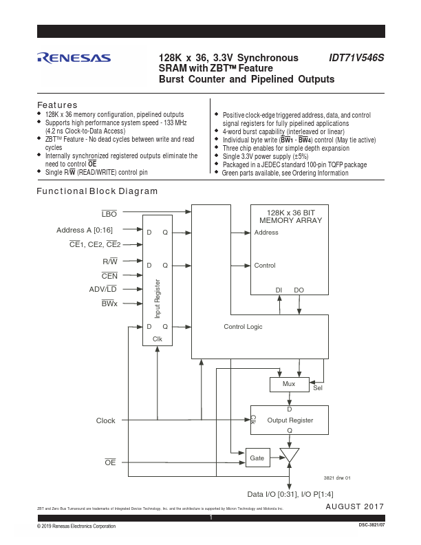
- Single R/W (READ/WRITE) control pin Functional Block Diagram LBO Address A [0:16] CE1, CE2, CE2