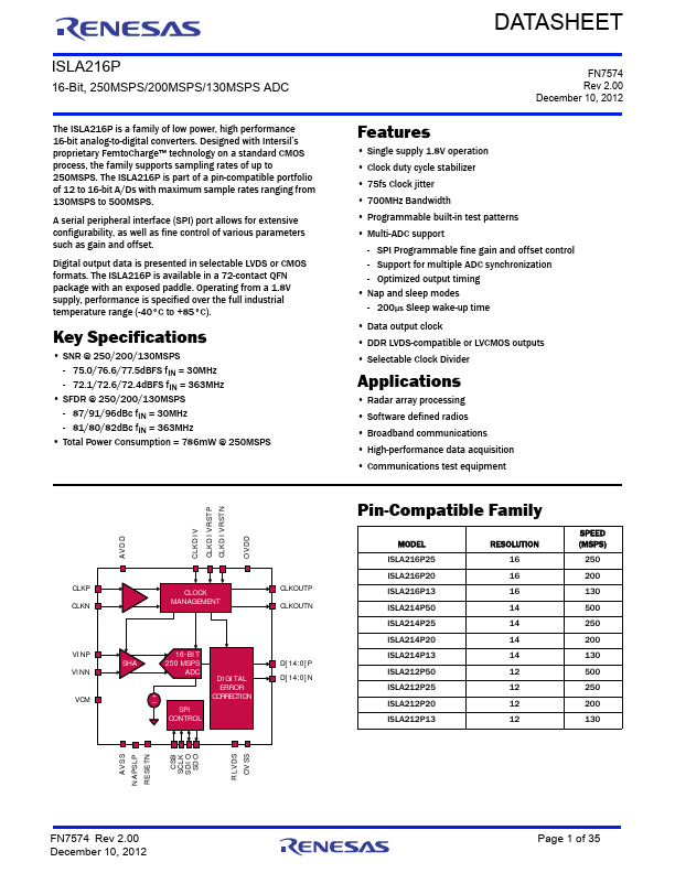
ISLA216P Description
ISLA216P 16-Bit, 250MSPS/200MSPS/130MSPS ADC The ISLA216P is a family of low power, high performance 16-bit analog-to-digital converters. Designed with Intersil’s proprietary FemtoCharge™ technology on a standard CMOS process, the family supports sampling rates of up to 250MSPS. The ISLA216P is part of a pin-patible portfolio of 12 to 16-bit A/Ds with maximum sample rates ranging from 130MSPS to 500MSPS.
ISLA216P Key Features
- Single supply 1.8V operation
- Clock duty cycle stabilizer
- 75fs Clock jitter
- 700MHz Bandwidth
- Programmable built-in test patterns
- Multi-ADC support
- SPI Programmable fine gain and offset control
- Support for multiple ADC synchronization
- Optimized output timing
- Nap and sleep modes