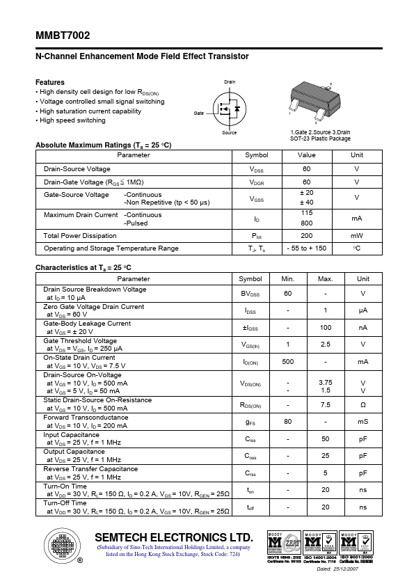
High speed switching
Gate
Absolute Maximum Ratings (Ta = 25 OC) Parameter
Drain-Source Voltage
Drain-Gate Voltage (RGS ≤ 1MΩ)
Gate-Source Voltage
-Continuous -Non Repetitive (tp < 50 µs)
Maximum Drain Current -Continuous -Pulsed
Total Power Dissipation
Operating and Storage Temperature Range
Drain
Source
Symbol VDSS VDGR VGSS ID P.
Full PDF Text Transcription for MMBT7002 (Reference)
Note: Below is a high-fidelity text extraction (approx. 800 characters) for
MMBT7002. For precise diagrams, and layout, please refer to the original PDF.
MMBT7002 N-Channel Enhancement Mode Field Effect Transistor Features • High density cell design for low RDS(ON) • Voltage controlled small signal switching • High saturat...
View more extracted text
low RDS(ON) • Voltage controlled small signal switching • High saturation current capability • High speed switching Gate Absolute Maximum Ratings (Ta = 25 OC) Parameter Drain-Source Voltage Drain-Gate Voltage (RGS ≤ 1MΩ) Gate-Source Voltage -Continuous -Non Repetitive (tp < 50 µs) Maximum Drain Current -Continuous -Pulsed Total Power Dissipation Operating and Storage Temperature Range Drain Source Symbol VDSS VDGR VGSS ID Ptot TJ, Ts 1.Gate 2.Source 3.