SFF24N50Z
SFF24N50Z is N-Channel Power MOSFET manufactured by SSDI.
- Part of the SFF24N50M comparator family.
- Part of the SFF24N50M comparator family.
Features
:
Rugged Construction with Polysilicon Gate Cell Low RDS(ON) and High Transconductance Excellent High Temperature Stability Very Fast Switching Speed Fast Recovery and Superior d V/dt Performance Increased Reverse Energy Capability Low Input and Transfer Capacitance for Easy Paralleling Ceramic Seals for Improved Hermeticity Hermetically Sealed Surface Mount Power Package TX, TXV, Space Level Screening Available Replacement for IXTH24N50 Types
Z = TO-254Z
- -
- -
- -
- -
- -
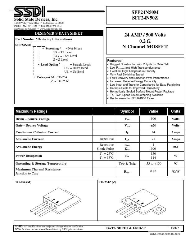
- Maximum Ratings
Drain
- Source Voltage Gate
- Source Voltage Continuous Collector Current Avalanche Current Avalanche Energy Power Dissipation Operating & Storage Temperature Maximum Thermal Resistance Junction to Case
TO-254 (M) TO-254Z (Z)
Symbol
VDS VGS ID Repetitive Repetitive Single Pulse TC = 25ºC TC = 55ºC IAR EAR EAS PD Top & Tstg RθJC
Value
500 ±20 24 21 1 690 150 114 -55 to +150 0.83
Units
Volts Volts Amps Amps m J W ºC ºC/W
NOTE: All specifications are subject to change without notification. SCD's for these devices should be reviewed by SSDI prior to release.
DATA SHEET #: F00165F
..
Solid State Devices, Inc.
14830 Valley View Blvd
- La Mirada, Ca 90638 Phone: (562) 404-7855
- Fax: (562) 404-1773 ssdi@ssdi-power.
- .ssdi-power.
SFF24N50M SFF24N50Z
Electrical Characteristics @ T J = 25ºC (Unless Otherwise Specified)
Drain to Source Breakdown Voltage (VGS=0 V, ID=250 µA) Drain to Source On State Resistance (VGS=10 V, ID=50% Rated ID) On State Drain Current (VDS>ID(on) X RDS(on) Max, VGS=10V) Gate Threshold Voltage (VDS=VGS, ID= 4m A) Forward Transconductance (VDS>ID(on) X RDS(on) Max, IDS= 50% Rated ID) Zero Gate Voltage Drain Current (VDS=max rated voltage, VGS=0 V) (VDS=80% rated VDS, VGS=0 V, TA=125ºC) Gate to Source Leakage Forward Gate to Source Leakage Reverse Total Gate Charge Gate to Source Charge Gate to Drain Charge Turn on Delay Time Rise Time Turn on Delay Time Fall Time Diode Forward Voltage (IS= Rated ID, VGS=0 V, TJ=25ºC) Diode Reverse Recovery...