M74HC251
M74HC251 is 8 BIT SIPO SHIFT REGISTER manufactured by STMicroelectronics.
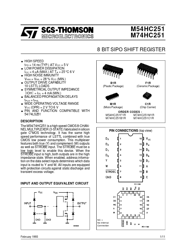
DESCRIPTION
The M54/74HC251 is a high speed CMOS 8-CHANNEL MULTIPLEXER (3-STATE) fabricated in silicon 2 gate C MOS technology. It has the same high speed performance of LSTTL bined with true CMOS low power consumption. This multiplexer features both true (Y) and plement (W) outputs as well as STROBE input. The STROBE must be a low logic level to enable this device. When the STROBE input is high, both outputs are in the high impedance state. When enabled, address information on the data select inputs determines which data input is routed to Y and W. All inputs are equipped with protection circuits against static discharge and transient excess voltage.
PIN CONNECTIONS (top view)
INPUT AND OUTPUT EQUIVALENT CIRCUIT
NC = No Internal Connection
February 1993
1/11
M54/M74HC251
TRUTH TABLE
INPUTS C X L L L L H H H H
X: Don’t Care Z: HIGH Impedance
OUTPUS A X L H L H L H L H STROBE S H L L L L L L L L Y Z D0 D1 D2 D3 D4 D5 D6 D7 W Z D0 D1 D2 D3 D4 D5 D6 D7
B X L L H H L L H H
LOGIC DIAGRAM
2/11
M54/M74HC251
PIN DESCRIPTION
PIN No 4, 3, 2, 1, 15, 14, 13, 12 5 6 7 11, 10, 9 8 16 SYMBOL D0 to D7 NAME AND FUNCTION Multiplexer Inputs
IEC LOGIC SYMBOL
Y W STROBE A, B, C GND V CC
Multiplexer Output plementary Multiplexer Output 3 State Output Enable Input Select Inputs Ground (0V) Positive Supply Voltage
ABSOLUTE MAXIMUM RATINGS
Symbol VCC VI VO IIK IOK IO ICC or IGND PD Tstg TL Parameter Supply Voltage DC Input Voltage DC Output Voltage DC Input Diode Current DC Output Diode Current DC Output Source Sink Current Per Output Pin DC VCC or Ground Current Power Dissipation Storage Temperature Lead Temperature (10 sec) Value -0.5 to +7 -0.5 to VCC + 0.5 -0.5 to VCC + 0.5 ± 20 ± 20 ± 25 ± 50 500 (- ) -65 to +150 300 Unit V V V m A m A m A m A m W o o
Absolute Maximum Ratings are those values beyond which damage to the device may occur. Functional operation under these condition isnotimplied. (- ) 500 m W: ≅ 65 o C derate to 300 m W by 10m W/o C: 65 o C to 85 o C
REMENDED...