STB16NK60Z-S Overview
Key Specifications
Max Operating Temp: 150 °C
Description
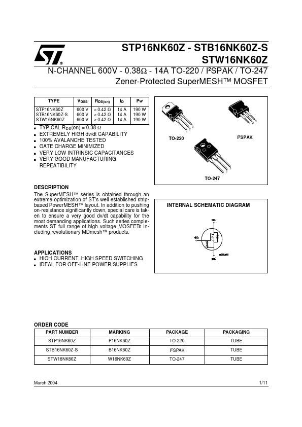
The SuperMESH™ series is obtained through an extreme optimization of ST’s well established stripbased PowerMESH™ layout. In addition to pushing on-resistance significantly down, special care is taken to ensure a very good dv/dt capability for the most demanding applications.