STB5NB60
STB5NB60 is N-CHANNEL POWER MOSFET manufactured by STMicroelectronics.
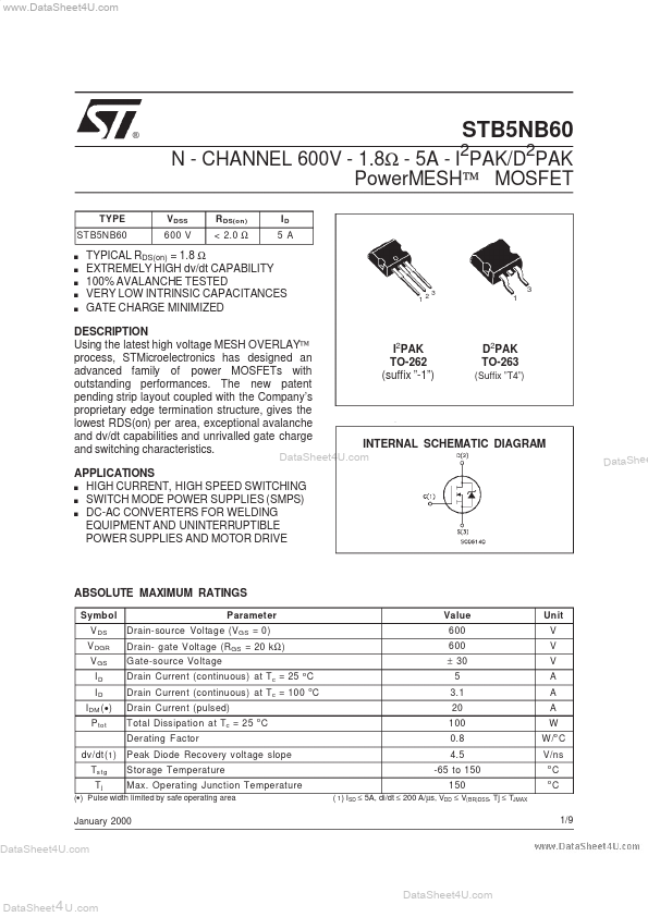
ON Using the latest high voltage MESH OVERLAY™ I2PAK D2PAK process, STMicroelectronics has designed an TO-262 TO-263 advanced family of power MOSFETs with (Suffix ”T4”) (suffix ”-1”) outstanding performances. The new patent pending strip layout coupled with the pany’s proprietary edge termination structure, gives the lowest RDS(on) per area, exceptional avalanche and dv/dt capabilities and unrivalled gate charge INTERNAL SCHEMATIC DIAGRAM and switching characteristics. . APPLICATIONS s HIGH CURRENT, HIGH SPEED SWITCHING s SWITCH MODE POWER SUPPLIES (SMPS) s DC-AC CONVERTERS FOR WELDING EQUIPMENT AND UNINTERRUPTIBLE POWER SUPPLIES AND MOTOR DRIVE
Data Shee
ABSOLUTE MAXIMUM RATINGS
Symbol V DS V DGR V GS ID ID I DM (
- ) P tot dv/dt( 1 ) Ts tg Tj Parameter Drain-source Voltage (V GS = 0) Drain- gate Voltage (R GS = 20 k Ω ) G ate-source Voltage Drain Current (continuous) at Tc = 25 C Drain Current (continuous) at Tc = 100 o C Drain Current (pulsed) T otal Dissipation at Tc = 25 o C Derating Factor Peak Diode Recovery voltage slope Storage Temperature Max. Operating Junction Temperature o
Value 600 600 ± 30 5 3.1 20 100 0.8 4.5 -65 to 150 150
( 1) ISD ≤ 5A, di/dt ≤ 200 A/µs, VDD ≤ V(BR)DSS, Tj ≤ TJMAX
Un it V V V A A A W W /o C V/ns o o
(- ) Pulse width limited by safe operating area
January 2000
1/9
.
. Data Sheet 4 U .
..
THERMAL DATA
R thj -case
Rthj -amb
R thc-sink Tl
Thermal Resistance Junction-case Max Thermal Resistance Junction-ambient Max Thermal Resistance Case-sink Typ Maximum Lead Temperature For Soldering Purpose
1.25 62.5 0.5 300
C/W o C/W o C/W o C o
AVALANCHE CHARACTERISTICS
Symbo l IAR E AS Parameter Avalanche Current, Repetitive or Not-Repetitive (pulse width limited by Tj max) Single Pulse Avalanche Energy o (starting Tj = 25 C, I D = IAR , VDD = 50 V) Max Valu e 5 300 Unit A m J
ELECTRICAL CHARACTERISTICS (Tcase = 25 o C unless otherwise specified) OFF
Symbo l V (BR)DSS I DSS IGSS Parameter Drain-source Breakdown Voltage...