STB60NF06L Overview
Key Specifications
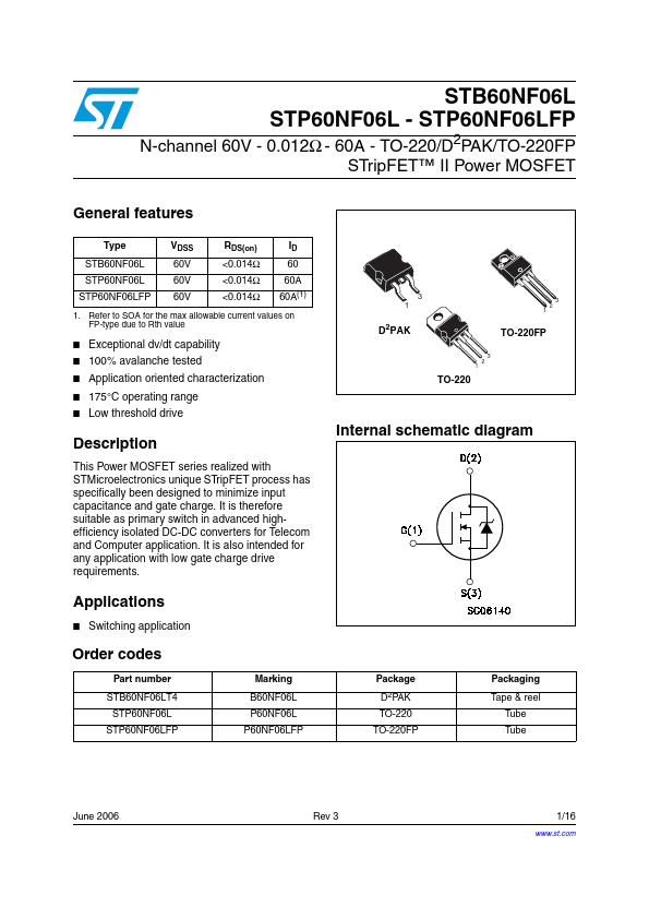
Package: D2PAK
Mount Type: Surface Mount
Pins: 3
Height: 4.6 mm
Key Features
- 60A TO-220/TO-220FP/D2PAK STripFET™ II POWER MOSFET
- ) Ptot dv/dt (1) EAS (2) VISO Tstg Tj
| Part | STB60NF06L |
|---|---|
| Description | N-CHANNEL Power MOSFET |
| Category | MOSFET |
| Manufacturer | STMicroelectronics |
| Size | 488.97 KB |
Package: D2PAK
Mount Type: Surface Mount
Pins: 3
Height: 4.6 mm
| Seller | Inventory | Price Breaks | Buy |
|---|---|---|---|
| Newark | 3663 | 1+ : 2.88 USD 10+ : 1.97 USD 25+ : 1.8 USD 50+ : 1.62 USD |
View Offer |
| Verical | 29000 | 1000+ : 0.7521 USD | View Offer |
| Part Number | Manufacturer | Description |
|---|---|---|
| STB60NF06LT4 | STMicroelectronics | N-CHANNEL POWER MOSFET |
| STB60NF06-1 | STMicroelectronics | N-CHANNEL Power MOSFET |