STD16NE10 Overview
Key Specifications
Max Operating Temp: 175 °C
Min Operating Temp: -55 °C
Description
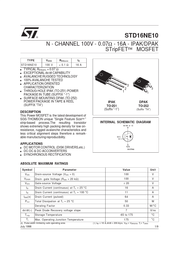
This Power MOSFET is the latest development of SGS-THOMSON unique ”Single Feature Size™ ” strip-based resulting transistor shows extremely high packing density for low onresistance, rugged avalanche characteristics and less critical alignment steps therefore a remarkable manufacturing reproducibility. APPLICATIONS s DC MOTOR CONTROL (DISK DRIVERS,etc.) s DC-DC & DC-ACCONVERTERS s SYNCHRONOUS RECTIFICATION Symbol V DS V DGR V GS ID ID IDM ( - ) P t ot Parameter Drain-source Voltage (V GS = 0) Drain- gate Voltage (R GS = 20 k Ω ) Gate-source Voltage Drain Current (continuous) at Tc = 25 C Drain Current (continuous) at Tc = 100 oC Drain Current (pulsed) Total Dissipation at Tc = 25 C Derating F actor dv/dt( 1 ) T stg Tj July 1998 Peak Diode Recovery voltage slope Storage T emperature Max.
Key Features
- ) P t ot Parameter Drain-source Voltage (V GS =
- ISD ≤ 16 A, di/dt ≤ 200 A/µs, VDD ≤ V(BR)DSS, Tj ≤ TJMAX Uni t V V V A A A W W/ o C V/ ns o o C C 1/9 (