STLC60133
STLC60133 is XDSL LINE DRIVER manufactured by STMicroelectronics.
XDSL LINE DRIVER
PRELIMINARY DATA s s s
LOW NOISE : 4n V/ H z HIGH PEAK OUTPUT CURRENT: 500 m A HIGH SPEED
- 140MHz Gain Bandwidth
- 30MHz Gain Flatness
- 400 V/us Slew Rate s
LOW POWER OPERATION
- ±5V to ±15V Voltage Supply
- 12.5 m A/Amp (typ) Supply current
- Power reduced Current
HTSSOP28 ORDERING NUMBER: STLC60133 Temperature Range: -40°C to +85°C s s s s
LOW SINGLE TONE DISTORTION THERMAL AND OVERLOAD PROTECTION HTSSOP28 PACKAGE -40 TO +85°C OPERATING RANGE Two digital pins (PWDN0 and PWDN1) allow the driver to work in full performance mode, in low-power mode or two intermediate bias states. The low-power mode biases the output stage in order to provide a low impedance at the amplifier outputs for back termination. The STLC60133 is designed optimizing bandwidth and distortion performances. For proper device operating it is necessary to work with a gain level greater than 15.6d B. Typical differential gain is normally +27d B, while typical mon mode gain is 15.6d B
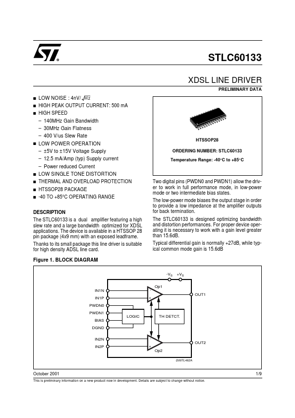
DESCRIPTION The STLC60133 is a dual amplifier featuring a high slew rate and a large bandwidth optimized for XDSL applications. The device is available in a HTSSOP 28 pin package (4x9 mm) with an exposed leadframe. Thanks to its small package this line driver is suitable for high density ADSL line card. Figure 1. BLOCK DIAGRAM
-VS Op1
+VS
IN1N IN1P PWDN0 PWDN1 BIAS DGND IN2N IN2P LOGIC
+
OUT1
TH DETCT.
+ Op2
D00TL462A
OUT2
October 2001
This is preliminary information on a new product now in development. Details are subject to change without notice.
1/9
PIN CONNECTION
RES N.C. N.C. IN2P IN2N OUT2 +VS +VS OUT1 IN1N IN1P N.C N.C. N.C.
1 2 3 4 5 6 7 8 9 10 11 12 13 14
D00TL463A
28 27 26 25 24 23 22 21 20 19 18 17 16...