Datasheet Details
| Part number | STW6NB100 |
|---|---|
| Manufacturer | STMicroelectronics |
| File Size | 86.74 KB |
| Description | N-CHANNEL MOSFET |
| Datasheet | STW6NB100_STMicroelectronics.pdf |
|
|
|
Overview: ® STW6NB100 N - CHANNEL 1000V - 2.3Ω - 5.4A - TO-247 PowerMESH™ MOSFET TYPE STW 6NB100 s s s s s s V DSS 1000 V R DS(on) < 2.8 Ω ID 5.4 A TYPICAL RDS(on) = 2.
| Part number | STW6NB100 |
|---|---|
| Manufacturer | STMicroelectronics |
| File Size | 86.74 KB |
| Description | N-CHANNEL MOSFET |
| Datasheet | STW6NB100_STMicroelectronics.pdf |
|
|
|
Using the latest high voltage technology, STMicroelectronics has designed an advanced family of power Mosfets with outstanding performances.
The new patent pending strip layout coupled with the Company’s proprietary edge termination structure, gives the lowest RDS(on) per area, exceptional avalanche and dv/dt capabilities and unrivalled gate charge and switching characteristics.
APPLICATIONS s HIGH CURRENT, HIGH SPEED SWITCHING s SWITCH MODE POWER SUPPLIES (SMPS) s DC-AC CONVERTERS FOR WELDING EQUIPMENT AND UNINTERRUPTIBLE POWER SUPPLIES AND MOTOR DRIVE
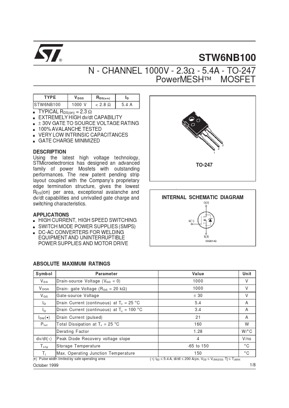
 TO-247 INTERNAL SCHEMATIC DIAGRAM ABSOLUTE MAXIMUM RATINGS Symb ol V DS V DGR V GS ID ID I DM ( • ) P tot dv/dt( 1 ) T s tg Tj Parameter Drain-source Voltage (VGS = 0) Drain- gate Voltage (RGS = 20 k Ω ) G ate-source Voltage Drain Current (continuous) at Tc = 25 C Drain Current (continuous) at Tc = 100 o C Drain Current (pulsed) T otal Dissipation at Tc = 25 C Derating F actor Peak Diode Recovery voltage slope Storage Temperature Max.
| Part Number | Description |
|---|---|
| STW6NB90 | N-CHANNEL MOSFET |
| STW6NA80 | N-CHANNEL MOSFET |
| STW6NA90 | N-CHANNEL MOSFET |
| STW6NC90Z | N-CHANNEL MOSFET |
| STW60N10 | N-CHANNEL MOSFET |
| STW60NE10 | N-CHANNEL MOSFET |
| STW10NA50 | N - CHANNEL ENHANCEMENT MODE FAST POWER MOS TRANSISTOR |
| STW10NB60 | N-CHANNEL Power MOSFET |
| STW10NC60 | N-CHANNEL Power MOSFET |
| STW10NC70Z | N-CHANNEL Power MOSFET |