HCF4099B
HCF4099B is 8-BIT ADDRESSABLE LATCH manufactured by STMicroelectronics.
HCC/HCF4099B
8-BIT ADDRESSABLE LATCH
- . . . .
SERIAL DATA INPUT
- ACTIVE PARALLEL OUTPUT STORAGE REGISTER CAPABILITY
- MASTER CLEAR CAN FUNCTION AS DEMULTIPLEXER STANDARDIZED SYMMETRICAL OUTPUT CHARACTERISTICS QUIESCENT CURRENT SPECIFIED TO 20V FOR HCC DEVICE 5V, 10V, AND 15V PARAMETRIC RATINGS INPUT CURRENT OF 100n A AT 18V AND 25°C FOR HCC DEVICE 100% TESTED FOR QUIESCENT CURRENT MEETS ALL REQUIREMENTS OF JEDEC TENTATIVE STANDARD N°. 13A, ”STANDARD SPECIFICATIONS FOR DESCRIPTION OF ”B” SERIES CMOS DEVICES”
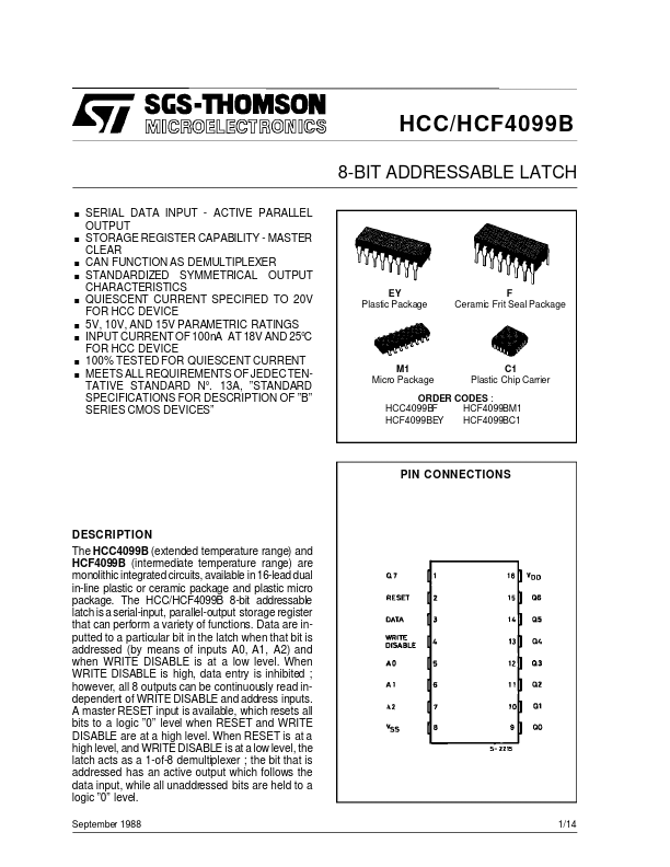
EY Plastic Package
F Ceramic Frit Seal Package
M1 Micro Package
C1 Plastic Chip Carrier
ORDER CODES : HCC4099BF HCF4099BM1 HCF4099BEY HCF4099BC1
PIN CONNECTIONS
DESCRIPTION The HCC4099B (extended temperature range) and HCF4099B (intermediate temperature range) are monolithic integrated circuits, available in 16-lead dual in-line plastic or ceramic package and plastic micro package. The HCC/HCF4099B 8-bit addressable latch is a serial-input, parallel-output storage register that can perform a variety of functions. Data are inputted to a particular bit in the latch when that bit is addressed (by means of inputs A0, A1, A2) and when WRITE DISABLE is at a low level. When WRITE DISABLE is high, data entry is inhibited ; however, all 8 outputs can be continuously read independent of WRITE DISABLE and address inputs. A master RESET input is available, which resets all bits to a logic ”0” level when RESET and WRITE DISABLE are at a high level. When RESET is at a high level, and WRITE DISABLE is at a low level, the latch acts as a 1-of-8 demultiplexer ; the bit that is addressed has an active output which follows the data input, while all unaddressed bits are held to a logic ”0” level.
September 1988 1/14
HCC/HCF4099B
FUNCTIONAL...