DESCRIPTION
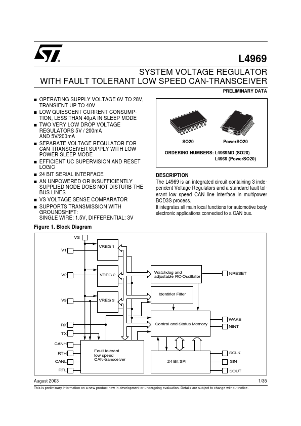
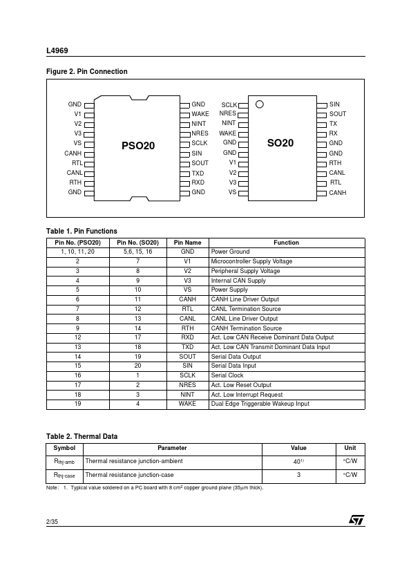
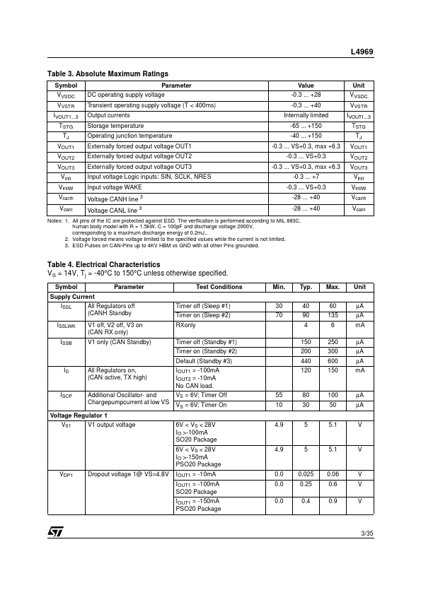
Figure 1. Block Diagram VS V1 VREG 1 V2 VREG 2 Watchdog and adjustable RC-Oscillator NRESET Identifier Filter V3 VREG 3 WAKE RX TX CANH RTH CANL RTL Fault tolerant low speed CAN-transceiver SCLK 24 Bit SPI SIN SOUT Control and Status Memory NINT August 2003 This is preliminary information on a new product now in development or undergoing evaluation. Details are subject to change without notice. 1/35 L4969 Figure 2. Pin Connection GND V1 V2 V3 VS CANH RTL CANL RTH GND GND WAKE NINT NRES SCLK NRES NINT WAKE GND GND V1 V2 V3 VS SIN SOUT TX RX PSO20 SCLK SIN SOUT TXD RXD GND SO20 GND GND RTH CANL RTL CANH Table 1. Pin Functions Pin No. (PSO20) 1, 10, 11, 20 2 3 4 5 6 7 8 9 12 13 14 15 16 17 18 19 Pin No. (SO20) 5,6, 15, 16 7 8 9 10 11 12 13 14 17 18 19 20 1 2 3 4 Pin Name GND V1 V2 V3 VS CANH RTL CANL RTH RXD TXD SOUT SIN SCLK NRES NINT WAKE Power Ground Microcontroller Supply Voltage Peripheral Supply Voltage Internal CAN Supply Power Supply CANH Line Driver Output CANL Termination Source CANL Line Driver Output CANH Termination Source Act. STMicroelectronics